- 您現(xiàn)在的位置:買賣IC網(wǎng) > PDF目錄372294 > ST24LC21BM6 IC CONFIG DEVICE 16MBIT 100-PQFP PDF資料下載
參數(shù)資料
| 型號(hào): | ST24LC21BM6 |
| 英文描述: | IC CONFIG DEVICE 16MBIT 100-PQFP |
| 中文描述: | I2C串行EEPROM的 |
| 文件頁數(shù): | 7/21頁 |
| 文件大小: | 152K |
| 代理商: | ST24LC21BM6 |

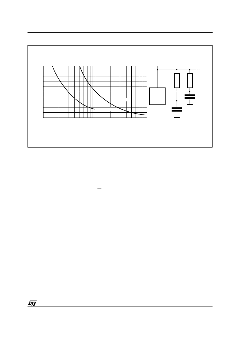
AI01665
VCC
CBUS
SDA
RL
MASTER
RL
SCL
CBUS
100
0
4
8
12
16
20
CBUS (pF)
M
)
10
1000
fc = 400kHz
fc = 100kHz
Figure 6. Maximum R
L
Value versus Bus Capacitance (C
BUS
) for an I
2
C Bus
Error Recovery Modes available in the
ST24FC21 and the ST24FW21
When the ST24FC21 (or the ST24FW21) first
switches to the I
2
C mode (VESA DDC2B mode), it
enters a transition state which is functionally iden-
tical to I
2
C operation. But, if the ST24FC21 (or the
ST24FW21) does not received a valid I
2
C se-
quence, that is a START condition followed by a
valid Device Select code (1010XXX RW), within
either 128 VCLK periods or a period of time of
t
RECOVERY
(approximately 2 seconds), the
ST24FC21 (or the ST24FW21) will revert to the
Transmit-Only mode (VESA DDC1 mode).
If the ST24FC21 (or the ST24FW21) decodes a
valid I
2
C Device Select code, it will lock into I
2
C
mode. Under this condition, signals applied on the
VCLK input will not disturb READ access from the
ST24FC21 (or the ST24FW21). For WRITE ac-
cess, refer to the Signal Description paragraph.
When in the transition state, the count of VCLK
pulses and the internal 2 seconds timer are reset
by any activity on the SCL line. This means that,
after each high to low transition on SCL, the mem-
ory will re-initialise its transition state and will switch
back to Transmit-Only mode only after 128 more
VCLK pulses or after a new t
RECOVERY
delay.
SIGNAL DESCRIPTIONS
I
2
C Serial Clock (SCL).
The SCL input pin is used
to synchronize all data in and out of the memory. A
resistor can be connected from the SCL line to V
CC
to act as a pull up (see Figure 6).
Serial Data (SDA).
The SDA pin is bi-directional
and is used to transfer data in or out of the memory.
It is an open drain output that may be wire-OR’ed
with other open drain or open collector signals on
the bus. A resistor must be connected from the SDA
bus line to V
CC
to act as pull up (see Figure 6).
Transmit Only Clock (VCLK)
. The VCLK input pin
is used to synchronize data out when the
ST24xy21 is in Transmit Only mode.
For the ST24LC21B and the ST24FC21 Only, the
VCLK offers also a Write Enable (active high) func-
tion when the ST24LC21B and the ST24FC21 are
in I
2
C bidirectional mode.
Write Control (WC).
An hardware Write Control
feature (WC) is offered only on ST24LW21 and
ST24FW21 on pin 3. This feature is usefull to
protect the contents of the memory from any erro-
neous erase/write cycle. The Write Control signal
is used to enable (WC = V
IL
) or disable (WC = V
IH
)
the internal write protection. When unconnected,
the WC input is internally tied to V
SS
by a 100k ohm
pull-down resistor and the memory is write pro-
tected.
7/21
ST24LC21B, ST24LW21, ST24FC21, ST24FW21
相關(guān)PDF資料 |
PDF描述 |
|---|---|
| ST24LW21B1 | IC CONFIG DEVICE 1.6MBIT 32-TQFP |
| ST24LW21B6 | IC CONFIG DEVICE 8MBIT 100-PQFP |
| ST24LW21M1 | Cyclone II FPGA 35K FBGA-672 |
| ST24LW21M6 | Cyclone II FPGA 15K FBGA-256 |
| ST24F | IC CONFIG DEVICE 16MBIT 100-PQFP |
相關(guān)代理商/技術(shù)參數(shù) |
參數(shù)描述 |
|---|---|
| ST24LC21BM6TR | 功能描述:電可擦除可編程只讀存儲(chǔ)器 Dual Mode 1K (128x8) RoHS:否 制造商:Atmel 存儲(chǔ)容量:2 Kbit 組織:256 B x 8 數(shù)據(jù)保留:100 yr 最大時(shí)鐘頻率:1000 KHz 最大工作電流:6 uA 工作電源電壓:1.7 V to 5.5 V 最大工作溫度:+ 85 C 安裝風(fēng)格:SMD/SMT 封裝 / 箱體:SOIC-8 |
| ST24LC21M1 | 制造商:未知廠家 制造商全稱:未知廠家 功能描述:I2C Serial EEPROM |
| ST24LC21M1TR | 制造商:STMICROELECTRONICS 制造商全稱:STMicroelectronics 功能描述:1Kb x8 DUAL MODE SERIAL EEPROM for VESA Plug&Play |
| ST24LW21 | 制造商:STMICROELECTRONICS 制造商全稱:STMicroelectronics 功能描述:1 Kbit x8 Dual Mode Serial EEPROM for VESA PLUG & PLAY |
| ST24LW21B1 | 制造商:未知廠家 制造商全稱:未知廠家 功能描述:I2C Serial EEPROM |
發(fā)布緊急采購,3分鐘左右您將得到回復(fù)。