- 您現(xiàn)在的位置:買賣IC網(wǎng) > PDF目錄372295 > ST24FC21M1 FPGA, FLEX 10K, 10K GATES, TQFP144; Logic IC family:FPGA; Logic IC Base Number:10; Logic IC function:EPF10K10; Voltage, supply:5.0V; Case style:TQFP; Gates, No. of:10000; I/O lines, No. of:102; Pins, No. of:144; Temp, op. RoHS Compliant: Yes PDF資料下載
參數(shù)資料
| 型號(hào): | ST24FC21M1 |
| 英文描述: | FPGA, FLEX 10K, 10K GATES, TQFP144; Logic IC family:FPGA; Logic IC Base Number:10; Logic IC function:EPF10K10; Voltage, supply:5.0V; Case style:TQFP; Gates, No. of:10000; I/O lines, No. of:102; Pins, No. of:144; Temp, op. RoHS Compliant: Yes |
| 中文描述: | I2C串行EEPROM的 |
| 文件頁(yè)數(shù): | 15/21頁(yè) |
| 文件大小: | 152K |
| 代理商: | ST24FC21M1 |
第1頁(yè)第2頁(yè)第3頁(yè)第4頁(yè)第5頁(yè)第6頁(yè)第7頁(yè)第8頁(yè)第9頁(yè)第10頁(yè)第11頁(yè)第12頁(yè)第13頁(yè)第14頁(yè)當(dāng)前第15頁(yè)第16頁(yè)第17頁(yè)第18頁(yè)第19頁(yè)第20頁(yè)第21頁(yè)

S
S
BYTE WRITE
CONTROL
BYTE
WORD ADDR
DATA
S
PAGE WRITE
WORD ADD n
DATA n
DATA n + 1
AI01894
ACK
ACK
ACK
ACK
ACK
ACK
VCLK/WC
CONTROL
BYTE
DATA n + 7
S
ACK
ACK
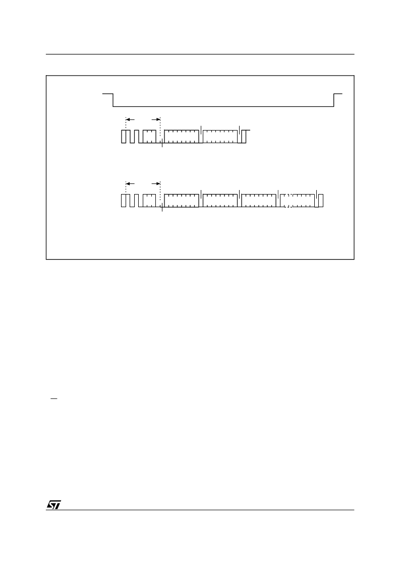
Figure 12. Inhibited Write when VCLK/WC = 0
– Step 2: if the memory is busy with the internal
write cycle, no ACK will be returned and the
master goes back to Step 1. If the memory
has terminated the internal write cycle, it will
respond with an ACK, indicating that the mem-
ory is ready to receive the second part of the
instruction (the first byte of this instruction was
already sent during Step 1).
Read Operations
On delivery, the memory content is set at all "1’s"
(or FFh).
Current Address Read.
The memory has an inter-
nal byte address counter. Each time a byte is read,
this counter is incremented. For the Current Ad-
dress Read mode, following a START condition,
the master sends the Device Select code with the
RW bit set to ’1’. The memory acknowledges this
and outputs the data byte addressed by the internal
byte address counter. This counter is then incre-
mented. The master must NOT acknowledge the
data byte output and terminates the transfer with a
STOP condition.
Random Address Read.
A dummy write is per-
formed to load the address into the address
counter, see Figure 14. This is followed by a Re-
START condition send by the master and the De-
vice Select code is repeated with the RW bit set to
’1’. The memory acknowledges this and outputs the
addressed data byte. The master must NOT ac-
knowledge the data byte output and terminates the
transfer with a STOP condition.
Sequential Read.
This mode can be initiated with
either a Current Address Read or a Random Ad-
dress Read. However, in this case the master
DOES acknowledge the data byte output and the
memory continues to output the next byte in se-
quence. To terminate the stream of bytes, the
master must NOT acknowledge the last data byte
output, and MUST generate a STOP condition.
The output data is from consecutive byte ad-
dresses, with the internal byte address counter
automatically incremented after each byte output.
After a count of the last memory address, the
address counter will ’roll-over’ and the memory will
continue to output data.
Acknowledge in Read Mode.
In all read modes
the ST24xy21 wait for an acknowledge during the
9th bit time. If the master does not pull the SDA line
low during this time, the ST24xy21 terminate the
data transfer and switches to a standby state.
15/21
ST24LC21B, ST24LW21, ST24FC21, ST24FW21
相關(guān)PDF資料 |
PDF描述 |
|---|---|
| ST24FC21M6 | IC ACEX 1K FPGA 100K 208-PQFP |
| ST24FW21B1 | IC ACEX 1K FPGA 100K 484-FBGA |
| ST24FW21B6 | IC MAX 7000 CPLD 32 44-PLCC |
| ST24LC21B1 | Stratix II FPGA 180K FBGA-1508 |
| ST24LC21M1 | IC CONFIG DEVICE 1.6MBIT 20-PLCC |
相關(guān)代理商/技術(shù)參數(shù) |
參數(shù)描述 |
|---|---|
| ST24FC21M1TR | 制造商:STMICROELECTRONICS 制造商全稱:STMicroelectronics 功能描述:1 Kbit x8 Dual Mode Serial EEPROM for VESA PLUG & PLAY |
| ST24FC21M6 | 功能描述:電可擦除可編程只讀存儲(chǔ)器 Dual Mode 1K (128x8) RoHS:否 制造商:Atmel 存儲(chǔ)容量:2 Kbit 組織:256 B x 8 數(shù)據(jù)保留:100 yr 最大時(shí)鐘頻率:1000 KHz 最大工作電流:6 uA 工作電源電壓:1.7 V to 5.5 V 最大工作溫度:+ 85 C 安裝風(fēng)格:SMD/SMT 封裝 / 箱體:SOIC-8 |
| ST24FC21M6TR | 功能描述:電可擦除可編程只讀存儲(chǔ)器 Dual Mode 1K (128x8) RoHS:否 制造商:Atmel 存儲(chǔ)容量:2 Kbit 組織:256 B x 8 數(shù)據(jù)保留:100 yr 最大時(shí)鐘頻率:1000 KHz 最大工作電流:6 uA 工作電源電壓:1.7 V to 5.5 V 最大工作溫度:+ 85 C 安裝風(fēng)格:SMD/SMT 封裝 / 箱體:SOIC-8 |
| ST24FW21 | 制造商:STMICROELECTRONICS 制造商全稱:STMicroelectronics 功能描述:1 Kbit x8 Dual Mode Serial EEPROM for VESA PLUG & PLAY |
| ST24FW21B1 | 制造商:未知廠家 制造商全稱:未知廠家 功能描述:I2C Serial EEPROM |
發(fā)布緊急采購(gòu),3分鐘左右您將得到回復(fù)。