- 您現(xiàn)在的位置:買賣IC網(wǎng) > PDF目錄365719 > SST39VF6401-90-4C-EKE (SILICON STORAGE TECHNOLOGY INC) 64 Mbit (x16) Multi-Purpose Flash Plus PDF資料下載
參數(shù)資料
| 型號(hào): | SST39VF6401-90-4C-EKE |
| 廠商: | SILICON STORAGE TECHNOLOGY INC |
| 元件分類: | PROM |
| 英文描述: | 64 Mbit (x16) Multi-Purpose Flash Plus |
| 中文描述: | 4M X 16 FLASH 2.7V PROM, 90 ns, PDSO48 |
| 封裝: | 12 X 20 MM, MO-142DD, TSOP1-48 |
| 文件頁數(shù): | 3/29頁 |
| 文件大小: | 474K |
| 代理商: | SST39VF6401-90-4C-EKE |
第1頁第2頁當(dāng)前第3頁第4頁第5頁第6頁第7頁第8頁第9頁第10頁第11頁第12頁第13頁第14頁第15頁第16頁第17頁第18頁第19頁第20頁第21頁第22頁第23頁第24頁第25頁第26頁第27頁第28頁第29頁
Preliminary Specifications
16 Mbit Multi-Purpose Flash Plus
SST39VF1681 / SST39VF1682
3
2003 Silicon Storage Technology, Inc.
S71243-03-000
11/03
Chip-Erase Operation
The SST39VF168x provide a Chip-Erase operation, which
allows the user to erase the entire memory array to the “1”
state. This is useful when the entire device must be quickly
erased.
The Chip-Erase operation is initiated by executing a six-
byte command sequence with Chip-Erase command
(10H) at address AAAH in the last byte sequence. The
Erase operation begins with the rising edge of the sixth
WE# or CE#, whichever occurs first. During the Erase
operation, the only valid read is Toggle Bit or Data# Polling.
See Table 6 for the command sequence, Figure 9 for tim-
ing diagram, and Figure 23 for the flowchart. Any com-
mands issued during the Chip-Erase operation are
ignored. When WP# is low, any attempt to Chip-Erase will
be ignored. During the command sequence, WP# should
be statically held high or low.
Write Operation Status Detection
The SST39VF168x provide two software means to detect
the completion of a Write (Program or Erase) cycle, in
order to optimize the system write cycle time. The software
detection includes two status bits: Data# Polling (DQ
7
) and
Toggle Bit (DQ
6
). The End-of-Write detection mode is
enabled after the rising edge of WE#, which initiates the
internal Program or Erase operation.
The actual completion of the nonvolatile write is asyn-
chronous with the system; therefore, either a Data# Poll-
ing or Toggle Bit read may be simultaneous with the
completion of the write cycle. If this occurs, the system
may possibly get an erroneous result, i.e., valid data may
appear to conflict with either DQ
7
or DQ
6
. In order to pre-
vent spurious rejection, if an erroneous result occurs, the
software routine should include a loop to read the
accessed location an additional two (2) times. If both
reads are valid, then the device has completed the Write
cycle, otherwise the rejection is valid.
Data# Polling (DQ
7
)
When the SST39VF168x are in the internal Program oper-
ation, any attempt to read DQ
7
will produce the comple-
ment of the true data. Once the Program operation is
completed, DQ
7
will produce true data. Note that even
though DQ
7
may have valid data immediately following the
completion of an internal Write operation, the remaining
data outputs may still be invalid: valid data on the entire
data bus will appear in subsequent successive Read
cycles after an interval of 1 μs. During internal Erase oper-
ation, any attempt to read DQ
7
will produce a ‘0’. Once the
internal Erase operation is completed, DQ
7
will produce a
‘1’. The Data# Polling is valid after the rising edge of fourth
WE# (or CE#) pulse for Program operation. For Sector-,
Block- or Chip-Erase, the Data# Polling is valid after the
rising edge of sixth WE# (or CE#) pulse. See Figure 6 for
Data# Polling timing diagram and Figure 20 for a flowchart.
Toggle Bits (DQ6 and DQ2)
During the internal Program or Erase operation, any con-
secutive attempts to read DQ
6
will produce alternating “1”s
and “0”s, i.e., toggling between 1 and 0. When the internal
Program or Erase operation is completed, the DQ
6
bit will
stop toggling. The device is then ready for the next opera-
tion. For Sector-, Block-, or Chip-Erase, the toggle bit (DQ
6
)
is valid after the rising edge of sixth WE# (or CE#) pulse.
DQ
6
will be set to “1” if a Read operation is attempted on an
Erase-Suspended Sector/Block. If Program operation is ini-
tiated in a sector/block not selected in Erase-Suspend
mode, DQ
6
will toggle.
An additional Toggle Bit is available on DQ
2
, which can be
used in conjunction with DQ
6
to check whether a particular
sector is being actively erased or erase-suspended. Table 1
shows detailed status bits information. The Toggle Bit
(DQ
2
) is valid after the rising edge of the last WE# (or CE#)
pulse of Write operation. See Figure 7 for Toggle Bit timing
diagram and Figure 20 for a flowchart.
Note:
DQ
7
and DQ
2
require a valid address when reading
status information.
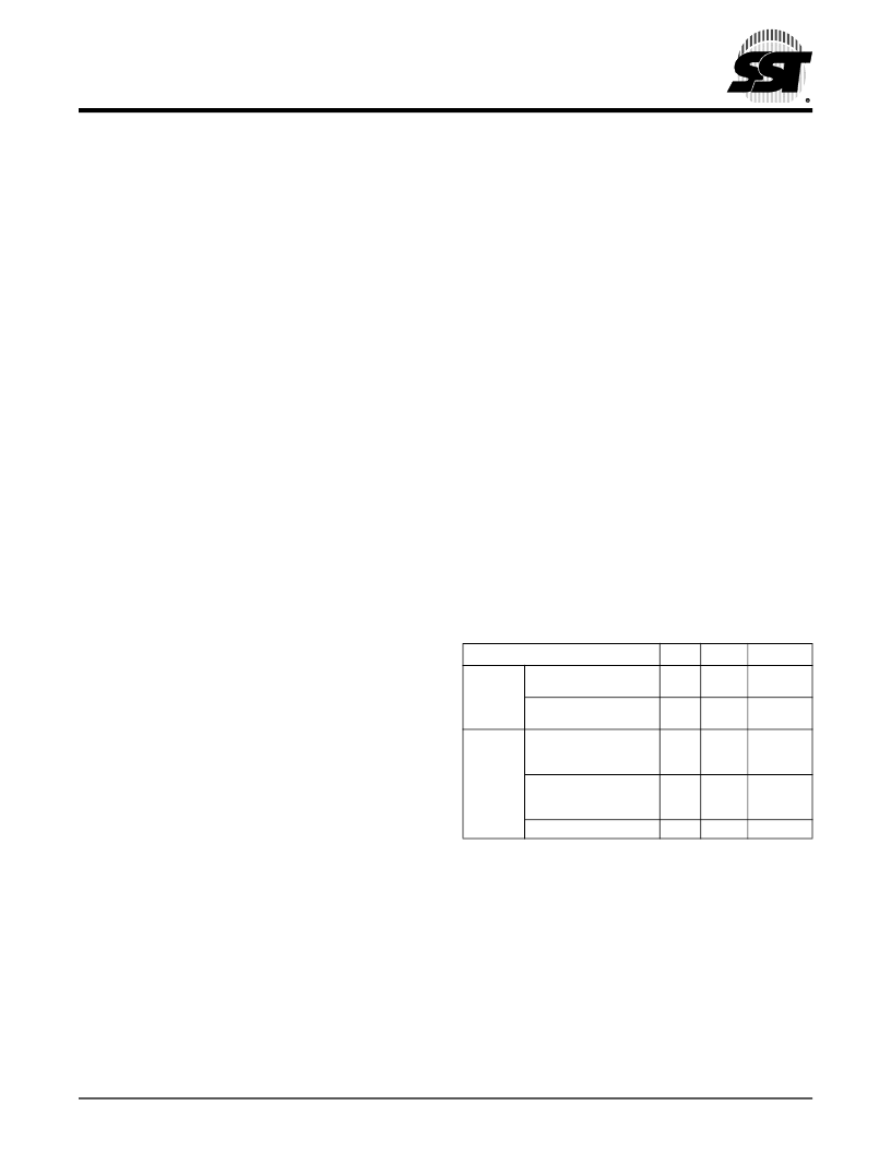
TABLE
1: W
RITE
O
PERATION
S
TATUS
Status
Normal
Operation
DQ
7
DQ
7
#
DQ
6
Toggle
DQ
2
Standard
Program
Standard
Erase
Read from
Erase Suspended
Sector/Block
Read from
Non- Erase Suspended
Sector/Block
Program
No Toggle
0
Toggle
Toggle
Erase-
Suspend
Mode
1
1
Toggle
Data
Data
Data
DQ
7
#
Toggle
N/A
T1.0 1243
相關(guān)PDF資料 |
PDF描述 |
|---|---|
| SST39VF6401-90-4I-B1K | 64 Mbit (x16) Multi-Purpose Flash Plus |
| SST39VF6401-90-4I-B1KE | SCOPEMETER 200MHz, 2.5GS/s,B/W with SCC kit, Z540 CALIBRATION RoHS Compliant: NA |
| SST39VF6401-90-4I-EK | 64 Mbit (x16) Multi-Purpose Flash Plus |
| SST39VF6401-90-4I-EKE | 64 Mbit (x16) Multi-Purpose Flash Plus |
| SST39VF6402 | 64 Mbit (x16) Multi-Purpose Flash Plus |
相關(guān)代理商/技術(shù)參數(shù) |
參數(shù)描述 |
|---|---|
| SST39VF6401B-70-4C-B1KE | 功能描述:閃存 64M (4Mx16) 70ns 2.7-3.6V Commercial RoHS:否 制造商:ON Semiconductor 數(shù)據(jù)總線寬度:1 bit 存儲(chǔ)類型:Flash 存儲(chǔ)容量:2 MB 結(jié)構(gòu):256 K x 8 定時(shí)類型: 接口類型:SPI 訪問時(shí)間: 電源電壓-最大:3.6 V 電源電壓-最小:2.3 V 最大工作電流:15 mA 工作溫度:- 40 C to + 85 C 安裝風(fēng)格:SMD/SMT 封裝 / 箱體: 封裝:Reel |
| SST39VF6401B-70-4C-B1KE-T | 功能描述:閃存 2.7 to 3.6V 64Mbit Multi-Purpose 閃存 RoHS:否 制造商:ON Semiconductor 數(shù)據(jù)總線寬度:1 bit 存儲(chǔ)類型:Flash 存儲(chǔ)容量:2 MB 結(jié)構(gòu):256 K x 8 定時(shí)類型: 接口類型:SPI 訪問時(shí)間: 電源電壓-最大:3.6 V 電源電壓-最小:2.3 V 最大工作電流:15 mA 工作溫度:- 40 C to + 85 C 安裝風(fēng)格:SMD/SMT 封裝 / 箱體: 封裝:Reel |
| SST39VF6401B-70-4C-EKE | 功能描述:閃存 64M (4Mx16) 70ns 2.7-3.6V Commercial RoHS:否 制造商:ON Semiconductor 數(shù)據(jù)總線寬度:1 bit 存儲(chǔ)類型:Flash 存儲(chǔ)容量:2 MB 結(jié)構(gòu):256 K x 8 定時(shí)類型: 接口類型:SPI 訪問時(shí)間: 電源電壓-最大:3.6 V 電源電壓-最小:2.3 V 最大工作電流:15 mA 工作溫度:- 40 C to + 85 C 安裝風(fēng)格:SMD/SMT 封裝 / 箱體: 封裝:Reel |
| SST39VF6401B-70-4C-EKE-T | 功能描述:閃存 2.7 to 3.6V 64Mbit Multi-Purpose 閃存 RoHS:否 制造商:ON Semiconductor 數(shù)據(jù)總線寬度:1 bit 存儲(chǔ)類型:Flash 存儲(chǔ)容量:2 MB 結(jié)構(gòu):256 K x 8 定時(shí)類型: 接口類型:SPI 訪問時(shí)間: 電源電壓-最大:3.6 V 電源電壓-最小:2.3 V 最大工作電流:15 mA 工作溫度:- 40 C to + 85 C 安裝風(fēng)格:SMD/SMT 封裝 / 箱體: 封裝:Reel |
| SST39VF6401B-70-4I-B1KE | 功能描述:閃存 64M (4Mx16) 70ns Industrial Temp RoHS:否 制造商:ON Semiconductor 數(shù)據(jù)總線寬度:1 bit 存儲(chǔ)類型:Flash 存儲(chǔ)容量:2 MB 結(jié)構(gòu):256 K x 8 定時(shí)類型: 接口類型:SPI 訪問時(shí)間: 電源電壓-最大:3.6 V 電源電壓-最小:2.3 V 最大工作電流:15 mA 工作溫度:- 40 C to + 85 C 安裝風(fēng)格:SMD/SMT 封裝 / 箱體: 封裝:Reel |
發(fā)布緊急采購,3分鐘左右您將得到回復(fù)。