- 您現(xiàn)在的位置:買賣IC網(wǎng) > PDF目錄193598 > SPT7883SIR (FAIRCHILD SEMICONDUCTOR CORP) 1-CH 10-BIT PROPRIETARY METHOD ADC, PARALLEL ACCESS, PDSO28 PDF資料下載
參數(shù)資料
| 型號: | SPT7883SIR |
| 廠商: | FAIRCHILD SEMICONDUCTOR CORP |
| 元件分類: | ADC |
| 英文描述: | 1-CH 10-BIT PROPRIETARY METHOD ADC, PARALLEL ACCESS, PDSO28 |
| 封裝: | SSOP-28 |
| 文件頁數(shù): | 3/8頁 |
| 文件大小: | 230K |
| 代理商: | SPT7883SIR |
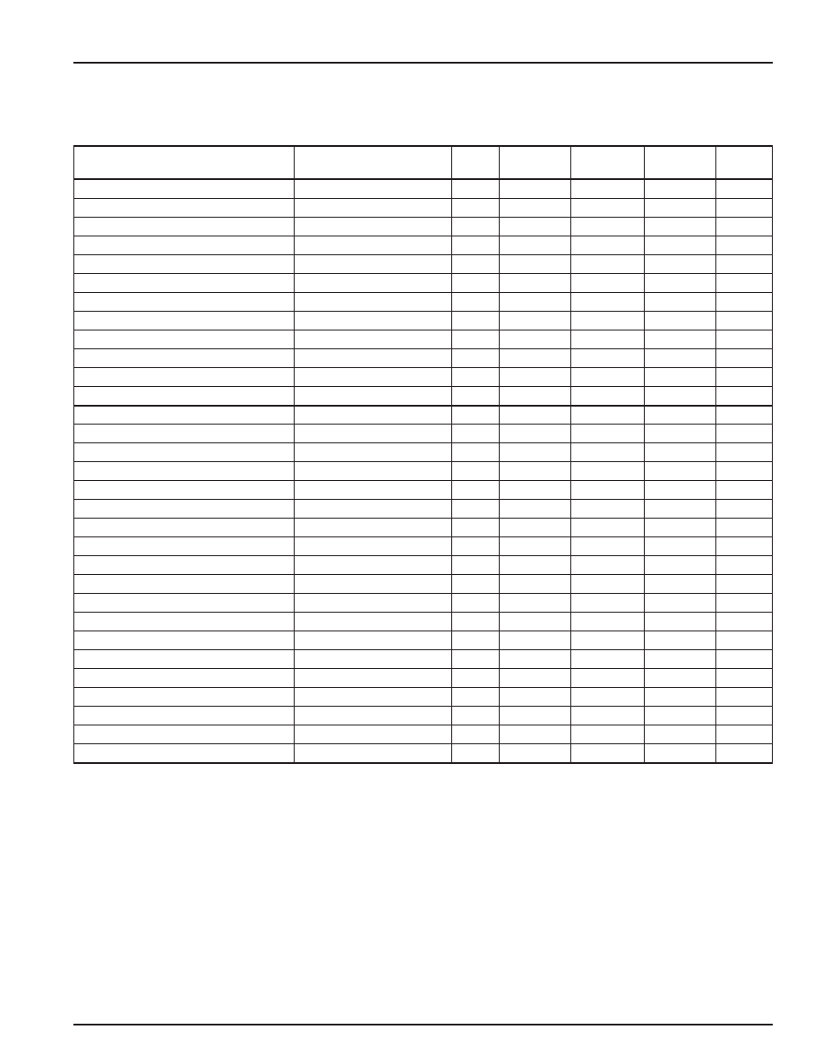
Parameter
Conditions
Test
Min.
Typ.
Max.
Unit
Level
Timing Characteristics
Max Conversion Rate
See graph pg 4
IV
70
MHz
Min Conversion Rate
IV
10
MHz
Pipeline Delay
See Timing Diag. pg 6
V
6
Cycles
Power Supply Requirements
Supply Voltage (VDD)IV
2.3
2.5
2.75
V
Output Driver Supply Voltage (OVDD)IV
1.75
2.5
2.75
V
Supply Current (IVDD + IOVDD)S = 70 MSPS;IN = 10MHz
I
52
64
mA
PSRR (Vos)
2.25V to 2.75V
V
60
dB
Power Dissipation
S = 70 MSPS;IN = 10MHz
I
129
160
mW
Sleep Mode Power Dissipation
S = 70 MSPS;IN = 10MHz
V
17
mW
Reference Voltages
Internal Ref Voltage Pos (VREFP)
EXTREF = 0
I
1.67
1.75
1.83
V
Internal Ref Voltage Neg (VREFN)
EXTREF = 0
I
0.67
0.75
0.83
V
Common Mode Output Voltage (VCM)I
1.17
1.25
1.33
V
Reference Temperature Coefficient
V
250
ppm/°C
External Positive Input Voltage
EXTREF = 1
IV
1.5
1.75
2.0
V
External Negative Input Voltage
EXTREF = 1
IV
0.5
0.75
1.0
V
Reference Input Voltage Range
IV
0.5
2.0
V
Digital Inputs
Logic “0” Voltage
I
0.5
V
Logic “1” Voltage
I
2.0
V
Logic “0” Current (VI = VGND)I
±10
A
Logic “1” Current (VI = VDD )I
±10
A
Digital Outputs
Logic “1” Voltage
I = -2mA
I
85% OVDD 90% OVDD
V
Logic “0” Voltage
I = 2mA
I
0.2
0.4
V
Timing Characteristics
CLK Fall to Output Data Valid (tD)CLOAD = 25 pF
IV
7.5
8.5
ns
Rise Time (tR)CLOAD = 25 pF
V
3.5
ns
Fall Time (tF)CLOAD = 25 pF
V
3.5
ns
NOTE: All electrical characteristics are subject to the following condition:
All parameters having min/max specifications are guaranteed. The Test Level column indicates the specific device testing actually performed
during production and quality assurance inspection. Any blank section in the data column indicates that the specification is not tested at the
specified condition.
TEST LEVEL CODES:
Level
Test Procedure
I
100% production tested at the specified temperature.
IV
Parameter is guaranteed (but not tested) by design and characterization data.
VParameter is a typical value for information purposes only.
SPT7883
DATA SHEET
Rev. 1a March 2003
3
Electrical Specifications
(TA = 25°C, VDD = OVDD = 2.5V, S = 70 MSPS, IN = 10MHz, internal references,
differential input signal, 50% duty cycle, typical bias; unless otherwise noted)
相關PDF資料 |
PDF描述 |
|---|---|
| SPT7920SCJ | 1-CH 12-BIT FLASH/SUCCESSIVE APPROXIMATION ADC, PARALLEL ACCESS, CDIP32 |
| SPT7920SCJ | 1-CH 12-BIT FLASH/SUCCESSIVE APPROXIMATION ADC, PARALLEL ACCESS, CDIP32 |
| SPT7920SCQ | 1-CH 12-BIT FLASH/SUCCESSIVE APPROXIMATION ADC, PARALLEL ACCESS, CQFP44 |
| SPT7921SCQ | 1-CH 12-BIT FLASH/SUCCESSIVE APPROXIMATION ADC, PARALLEL ACCESS, CQFP44 |
| SPT7930SCS | 1-CH 12-BIT RESISTANCE LADDER ADC, PARALLEL ACCESS |
相關代理商/技術參數(shù) |
參數(shù)描述 |
|---|---|
| SPT7910 | 制造商:未知廠家 制造商全稱:未知廠家 功能描述:12-BIT, 10 MSPS, ECL, A/D CONVERTER |
| SPT7910SCJ | 制造商:未知廠家 制造商全稱:未知廠家 功能描述:12-BIT, 10 MSPS, ECL, A/D CONVERTER |
| SPT7910SCU | 制造商:未知廠家 制造商全稱:未知廠家 功能描述:12-BIT, 10 MSPS, ECL, A/D CONVERTER |
| SPT7920 | 制造商:未知廠家 制造商全稱:未知廠家 功能描述:12-BIT, 10 MSPS, TTL, A/D CONVERTER |
| SPT7920SCJ | 制造商:未知廠家 制造商全稱:未知廠家 功能描述:12-BIT, 10 MSPS, TTL, A/D CONVERTER |
發(fā)布緊急采購,3分鐘左右您將得到回復。