- 您現(xiàn)在的位置:買賣IC網(wǎng) > PDF目錄225224 > SPT7840SCS (SIGNAL PROCESSING TECHNOLOGIES) 1-CH 10-BIT SUCCESSIVE APPROXIMATION ADC, PARALLEL ACCESS, PDSO28 PDF資料下載
參數(shù)資料
| 型號: | SPT7840SCS |
| 廠商: | SIGNAL PROCESSING TECHNOLOGIES |
| 元件分類: | ADC |
| 英文描述: | 1-CH 10-BIT SUCCESSIVE APPROXIMATION ADC, PARALLEL ACCESS, PDSO28 |
| 封裝: | SOIC-28 |
| 文件頁數(shù): | 12/12頁 |
| 文件大小: | 96K |
| 代理商: | SPT7840SCS |
SPT
9
2/10/98
SPT7840
CLOCK INPUT
The SPT7840 is driven from a single-ended TTL-input clock.
Because the pipelined architecture operates on the rising
edge of the clock input, the device can operate over a wide
range of input clock duty cycles without degrading the dy-
namic performance.
The device's sample rate is 1/2 of the
input clock frequency. (See the timing diagram.)
DIGITAL OUTPUTS
The digital outputs (D0-D10) are driven by a separate supply
(OVDD) ranging from +3 V to +5 V. This feature makes it
possible to drive the SPT7840's TTL/CMOS-compatible out-
puts with the user's logic system supply. The format of the
output data (D0-D9) is straight binary. (See table III.) The
outputs are latched on the rising edge of CLK. These outputs
can be switched into a tri-state mode by bringing EN high.
Table III - Output Data Information
ANALOG INPUT
OVERRANGE
OUTPUT CODE
D10
D9-D0
+F.S. + 1/2 LSB
1
11 1111 1111
+F.S. -1/2 LSB
O
11 1111 111
+1/2 F.S.
O
+1/2 LSB
O
OO OOOO OOO
0.0 V
O
OO OOOO OOOO
( indicates the flickering bit between logic 0 and 1).
OVERRANGE OUTPUT
The OVERRANGE OUTPUT (D10) is an indication that the
analog input signal has exceeded the positive full scale input
voltage by 1 LSB. When this condition occurs, D10 will switch
to logic 1. All other data outputs (D0 to D9) will remain at
logic 1 as long as D10 remains at logic 1. This feature makes
it possible to include the SPT7840 into higher resolution
systems.
EVALUATION BOARD
The EB7840 evaluation board is available to aid designers in
demonstrating the full performance of the SPT7840. This
board includes a reference circuit, clock driver circuit, output
data latches and an on-board reconstruction of the digital
data. An application note describing the operation of this
board as well as information on the testing of the SPT7840 is
also available. Contact the factory for price and availability.
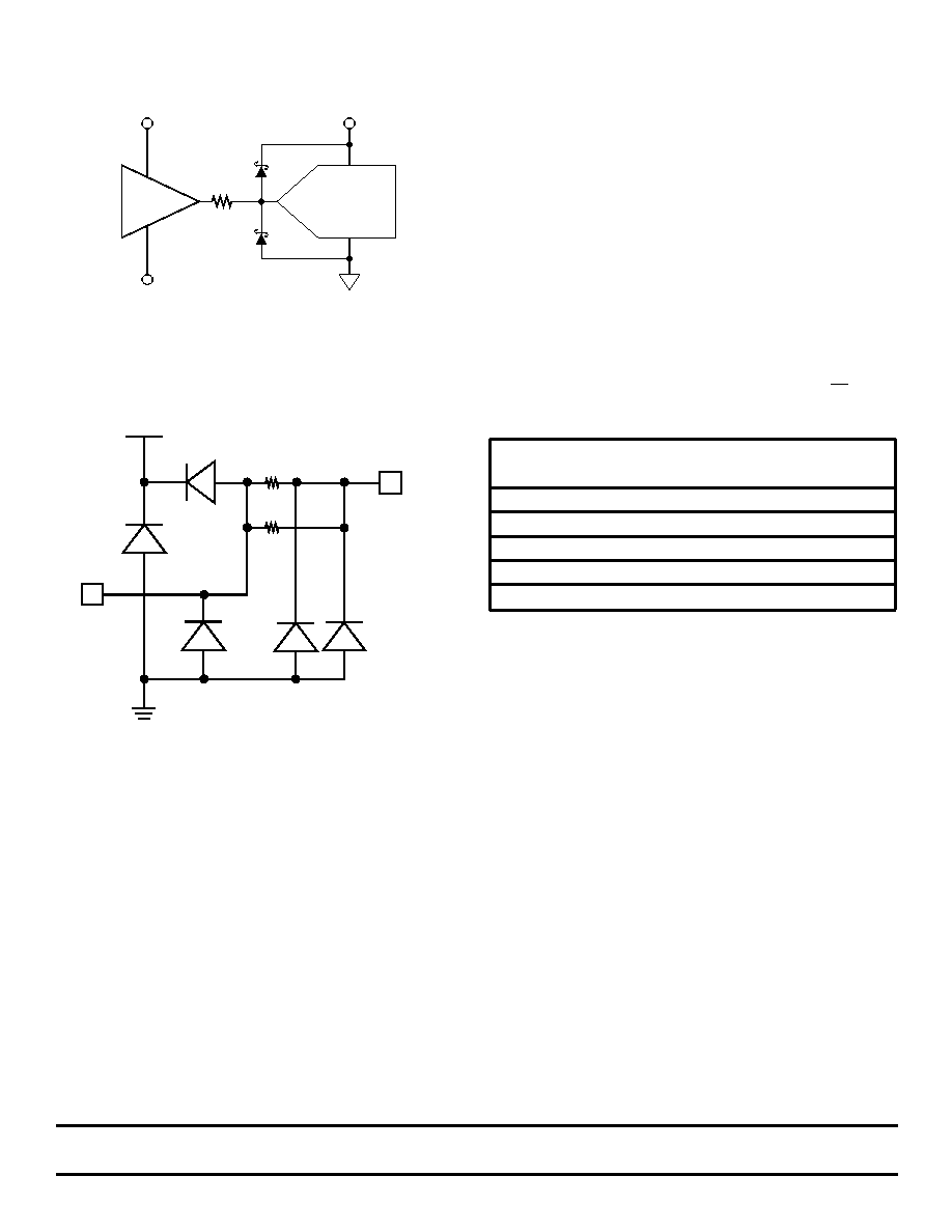
Figure 4 - Recommended Input Protection Circuit
47
D1
D2
ADC
Buffer
AVDD
+V
-V
D1 = D2 = Hewlett Packard HP5712 or equivalent
Figure 5 - On-Chip Protection Circuit
VDD
Analog
Pad
120
120
POWER SUPPLY SEQUENCING CONSIDERATIONS
All logic inputs should be held low until power to the device
has settled to the specific tolerances. Avoid power decou-
pling networks with large time constants which could delay
VDD power to the device.
相關(guān)PDF資料 |
PDF描述 |
|---|---|
| SPT7861SCU | 1-CH 10-BIT SUCCESSIVE APPROXIMATION ADC, PARALLEL ACCESS, UUC28 |
| SPT7862SIT | DUAL 1-CH 10-BIT SUCCESSIVE APPROXIMATION ADC, PARALLEL ACCESS, PQFP64 |
| SPT7862SIT | DUAL 1-CH 10-BIT SUCCESSIVE APPROXIMATION ADC, PARALLEL ACCESS, PQFP64 |
| SPT7866 | 1-CH 10-BIT PROPRIETARY METHOD ADC, PARALLEL ACCESS, PDSO28 |
| SPT7866 | 1-CH 10-BIT PROPRIETARY METHOD ADC, PARALLEL ACCESS, PDSO28 |
相關(guān)代理商/技術(shù)參數(shù) |
參數(shù)描述 |
|---|---|
| SPT7840SCT | 制造商:FAIRCHILD 制造商全稱:Fairchild Semiconductor 功能描述:10-BIT, 10 MSPS, 100 mW A/D CONVERTER |
| SPT7840SIS | 制造商:FAIRCHILD 制造商全稱:Fairchild Semiconductor 功能描述:10-BIT, 10 MSPS, 100 mW A/D CONVERTER |
| SPT7850 | 制造商:FAIRCHILD 制造商全稱:Fairchild Semiconductor 功能描述:10-BIT, 20 MSPS, 140 mW A/D CONVERTER |
| SPT7850SCN | 制造商:FAIRCHILD 制造商全稱:Fairchild Semiconductor 功能描述:10-BIT, 20 MSPS, 140 mW A/D CONVERTER |
| SPT7850SCT | 制造商:CADEKA 制造商全稱:CADEKA 功能描述:10-BIT, 20 MSPS, 140 mW A/D CONVERTER |
發(fā)布緊急采購,3分鐘左右您將得到回復(fù)。