- 您現(xiàn)在的位置:買賣IC網(wǎng) > PDF目錄69025 > SPAKMC332GVPV20 (FREESCALE SEMICONDUCTOR INC) 32-BIT, 20 MHz, MICROCONTROLLER, PQFP132 PDF資料下載
參數(shù)資料
| 型號(hào): | SPAKMC332GVPV20 |
| 廠商: | FREESCALE SEMICONDUCTOR INC |
| 元件分類: | 微控制器/微處理器 |
| 英文描述: | 32-BIT, 20 MHz, MICROCONTROLLER, PQFP132 |
| 封裝: | PLASTIC, QFP-132 |
| 文件頁數(shù): | 213/265頁 |
| 文件大?。?/td> | 6905K |
| 代理商: | SPAKMC332GVPV20 |
第1頁第2頁第3頁第4頁第5頁第6頁第7頁第8頁第9頁第10頁第11頁第12頁第13頁第14頁第15頁第16頁第17頁第18頁第19頁第20頁第21頁第22頁第23頁第24頁第25頁第26頁第27頁第28頁第29頁第30頁第31頁第32頁第33頁第34頁第35頁第36頁第37頁第38頁第39頁第40頁第41頁第42頁第43頁第44頁第45頁第46頁第47頁第48頁第49頁第50頁第51頁第52頁第53頁第54頁第55頁第56頁第57頁第58頁第59頁第60頁第61頁第62頁第63頁第64頁第65頁第66頁第67頁第68頁第69頁第70頁第71頁第72頁第73頁第74頁第75頁第76頁第77頁第78頁第79頁第80頁第81頁第82頁第83頁第84頁第85頁第86頁第87頁第88頁第89頁第90頁第91頁第92頁第93頁第94頁第95頁第96頁第97頁第98頁第99頁第100頁第101頁第102頁第103頁第104頁第105頁第106頁第107頁第108頁第109頁第110頁第111頁第112頁第113頁第114頁第115頁第116頁第117頁第118頁第119頁第120頁第121頁第122頁第123頁第124頁第125頁第126頁第127頁第128頁第129頁第130頁第131頁第132頁第133頁第134頁第135頁第136頁第137頁第138頁第139頁第140頁第141頁第142頁第143頁第144頁第145頁第146頁第147頁第148頁第149頁第150頁第151頁第152頁第153頁第154頁第155頁第156頁第157頁第158頁第159頁第160頁第161頁第162頁第163頁第164頁第165頁第166頁第167頁第168頁第169頁第170頁第171頁第172頁第173頁第174頁第175頁第176頁第177頁第178頁第179頁第180頁第181頁第182頁第183頁第184頁第185頁第186頁第187頁第188頁第189頁第190頁第191頁第192頁第193頁第194頁第195頁第196頁第197頁第198頁第199頁第200頁第201頁第202頁第203頁第204頁第205頁第206頁第207頁第208頁第209頁第210頁第211頁第212頁當(dāng)前第213頁第214頁第215頁第216頁第217頁第218頁第219頁第220頁第221頁第222頁第223頁第224頁第225頁第226頁第227頁第228頁第229頁第230頁第231頁第232頁第233頁第234頁第235頁第236頁第237頁第238頁第239頁第240頁第241頁第242頁第243頁第244頁第245頁第246頁第247頁第248頁第249頁第250頁第251頁第252頁第253頁第254頁第255頁第256頁第257頁第258頁第259頁第260頁第261頁第262頁第263頁第264頁第265頁
MC68332
SYSTEM INTEGRATION MODULE
USER’S MANUAL
4-11
ply must be used as the VDDSYN source. Adequate external bypass capacitors should
be placed as close as possible to the VDDSYN pin to assure stable operating frequen-
cy. When an external system clock signal is applied and the PLL is disabled, VDDSYN
should be connected to the VDD supply. Refer to the SIM Reference Manual (SIMRM/
AD) for more information regarding system clock power supply conditioning.
A voltage controlled oscillator (VCO) generates the system clock signal. To maintain
a 50% clock duty cycle, VCO frequency is either two or four times system clock fre-
quency, depending on the state of the X bit in SYNCR. A portion of the clock signal is
fed back to a divider/counter. The divider controls the frequency of one input to a
phase comparator. The other phase comparator input is a reference signal, either from
the crystal oscillator or from an external source. The comparator generates a control
signal proportional to the difference in phase between the two inputs. The signal is low-
pass filtered and used to correct VCO output frequency.
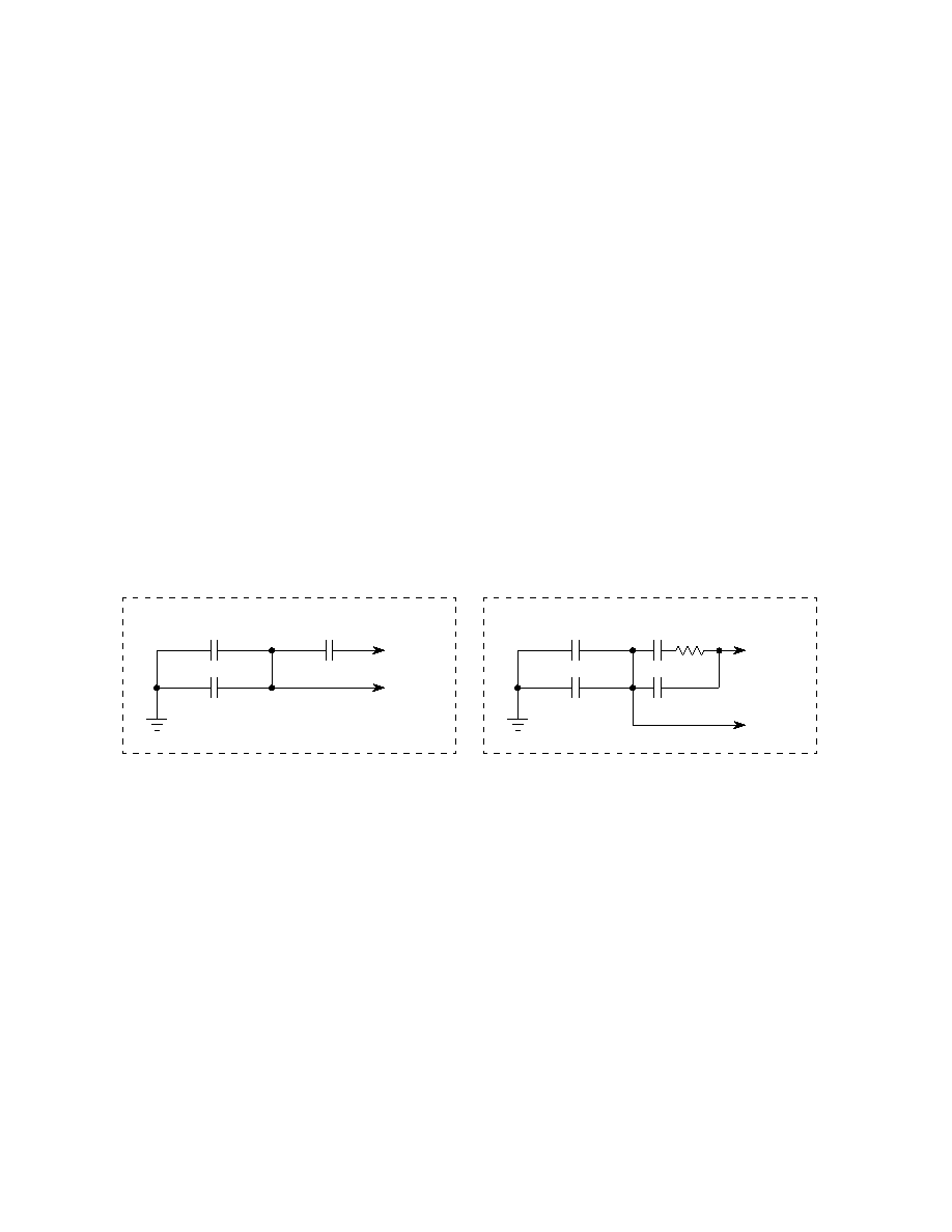
Filter geometry can vary, depending upon the external environment and required clock
stability. Figure 4-6 shows two recommended filters. XFC pin leakage must be as
specified in APPENDIX A ELECTRICAL CHARACTERISTICS to maintain optimum
stability and PLL performance.
An external filter network connected to the XFC pin is not required when an external
system clock signal is applied and the PLL is disabled. The XFC pin must be left float-
ing in this case.
Figure 4-6 System Clock Filter Networks
The synthesizer locks when VCO frequency is equal to EXTAL frequency. Lock time
is affected by the filter time constant and by the amount of difference between the two
comparator inputs. Whenever comparator input changes, the synthesizer must relock.
Lock status is shown by the SLOCK bit in SYNCR. During power-up, the MCU does
not come out of reset state until the synthesizer locks. Crystal type, characteristic fre-
quency, and layout of external oscillator circuitry affect lock time.
16/32 XFC CONN
1. Maintain low-leakage on the XFC node. See Appendix A electrical characteristics for more information.
2. Recommended loop filter for reduced sensitivity to low-frequency noise.
0.01
F
0.1
F
NORMAL OPERATING
ENVIRONMENT
HIGH-STABILITY OPERATING
ENVIRONMENT
C4
C1
VSSI
VDDSYN
XFC1
0.1
F
C3
0.01
F
0.1
F
C4
C1
VSSI
VDDSYN
XFC1, 2
0.1
F
C3
0.01
F
C2
18k
R1
F
re
e
sc
a
le
S
e
m
ic
o
n
d
u
c
to
r,
I
Freescale Semiconductor, Inc.
For More Information On This Product,
Go to: www.freescale.com
n
c
..
.
相關(guān)PDF資料 |
PDF描述 |
|---|---|
| MC68349FT16 | 32-BIT, MICROCONTROLLER, PQFP16 |
| MC68349FT25 | 32-BIT, MICROCONTROLLER, PQFP16 |
| MC68356CZP25 | 3 CHANNEL(S), 115K bps, SERIAL COMM CONTROLLER, PBGA357 |
| MC68356ZP25 | 3 CHANNEL(S), 115K bps, SERIAL COMM CONTROLLER, PBGA357 |
| MC6840L | 3 TIMER(S), PROGRAMMABLE TIMER, CDIP28 |
相關(guān)代理商/技術(shù)參數(shù) |
參數(shù)描述 |
|---|---|
| SPAKMC332MFC16 | 制造商:MOTOROLA 制造商全稱:Motorola, Inc 功能描述:32-Bit Modular Microcontroller |
| SPAKMC332MFC20 | 制造商:MOTOROLA 制造商全稱:Motorola, Inc 功能描述:32-Bit Modular Microcontroller |
| SPAKMC332MFV16 | 制造商:MOTOROLA 制造商全稱:Motorola, Inc 功能描述:32-Bit Modular Microcontroller |
| SPAKMC332MFV20 | 制造商:MOTOROLA 制造商全稱:Motorola, Inc 功能描述:32-Bit Modular Microcontroller |
| SPAKMC332VFC16 | 制造商:MOTOROLA 制造商全稱:Motorola, Inc 功能描述:32-Bit Modular Microcontroller |
發(fā)布緊急采購,3分鐘左右您將得到回復(fù)。