- 您現(xiàn)在的位置:買賣IC網(wǎng) > PDF目錄379399 > SP8855 (Mitel Networks Corporation) MOSFET; Transistor Polarity:N Channel; Drain Source Voltage, Vds:30V; Continuous Drain Current, Id:15A; On-Resistance, Rds(on):10mohm; Rds(on) Test Voltage, Vgs:10V; Package/Case:TO-252; Leaded Process Compatible:No PDF資料下載
參數(shù)資料
| 型號(hào): | SP8855 |
| 廠商: | Mitel Networks Corporation |
| 英文描述: | MOSFET; Transistor Polarity:N Channel; Drain Source Voltage, Vds:30V; Continuous Drain Current, Id:15A; On-Resistance, Rds(on):10mohm; Rds(on) Test Voltage, Vgs:10V; Package/Case:TO-252; Leaded Process Compatible:No |
| 中文描述: | 2.8GHz的并聯(lián)負(fù)載專業(yè)合成器 |
| 文件頁(yè)數(shù): | 11/14頁(yè) |
| 文件大?。?/td> | 169K |
| 代理商: | SP8855 |
第1頁(yè)第2頁(yè)第3頁(yè)第4頁(yè)第5頁(yè)第6頁(yè)第7頁(yè)第8頁(yè)第9頁(yè)第10頁(yè)當(dāng)前第11頁(yè)第12頁(yè)第13頁(yè)第14頁(yè)
11
SP8855E
A minimum value for the pull down resistor is 330 Ohms. When
the F
and
F
outputs are disabled the output level will be at
the logic low level of about 3.5V so that the additional supply
current due to the load resistors will be present even when the
outputs are disabled.
Reference input
The reference input circuit functions as an input amplifier or
crystal oscillator. When an external reference signal is used
this is simply AC coupled to pin 28, the base of the input
emitter follower. When a low phase noise synthesiser is
required the reference signal is critical since any noise present
here will be multiplied by the loop. To obtain the lowest
possible phase noise from the SP8855E it is best to use the
highest possible reference input frequency and to divide this
down internally to obtain the required frequency at the phase
detector. The amplitude of the reference input is also
important, and a level close to the maximum will give the
lowest noise. When the use of a low reference input frequency
say 4-10MHz is essential some advantage may be gained by
using a limiting amplifier such as a CMOS gate to square up
the reference input.
In cases where a suitable reference signal is not available,
it may be more convenient to use the input buffer as a crystal
oscillator in this case the emitter follower input transistor is
connected as a Colpitts oscillator with the crystal connected
from the base to ground and with the feedback necessary for
oscillation provided by a capacitor tap at the emitter. The
arrangement
is
shown
inset
in
Fig.
5.
FROM
CHARGE
PUMP
OUTPUT
FROM
CHARGE
PUMP
REFERENCE
C
1
C
2
R
2
TO
VCO
-
+
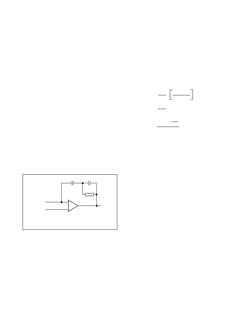
Fig. 8 third order loop filter circuit diagram
Loop Filter Design
Generally the third order filter configuration shown in Fig.8
gives better results than the more commonly used second
order because the reference sidebands are reduced. Three
equations are required to determine values for the three
constants where;
τ
1
= C
1
τ
2
= R
2
(C
1
+ C
2
)
τ
3
= C
2
R
2
The equations are
2
τ
2
=
1
2
τ
3
ω
n
3
τ
3
=
- tan
φ
ο
+
1
cos
ω
n
Where;
K
φ
K
0
N
is the phase detector gain factor in mA/radian
is theVCO gain factor in radian/second/Volt
is the total division ratio from VCO to reference
frequency
is the natural loop bandwidth
is the phase margin normally set to 45
°
Since the phase detector is linear over a range of 2
π
radian,
K
φ
can be calculated from
ω
n
φ
ο
K
φ
=
Phase comparator current setting/2
π
mA/radian
These values can now be substituted in equation 1 to obtain
a value for C
1
and equation 2 and 3 used to determine values
for C
2
and R
2
EXAMPLE
Calculate values for a loop with the following parameters
Frequency to be synthesised:
Reference frequency
Division ratio
ω
n
natural loop frequency
K
0
VCO gain factor
φ
0
phase margin
Phase comparator current
1000MHz
10MHz
1000MHz/10MHz = 100
100KHz
2
π
x 10MHz/Volt
45
°
6.3mA
The phase detector gain factor K
φ
= 6.3mA /2
π
= 1mA/radian
1
τ
1
=
K
φ
K
0
N
ω
n
2
1 +
ω
n
1 +
ω
n
2
τ
2
2
2
τ
3
2
1/2
φ
ο
相關(guān)PDF資料 |
PDF描述 |
|---|---|
| SP8855E | 2.8GHz Parallel Load Professional Synthesiser |
| SP8858 | 1·5GHz Professional Synthesiser |
| SP8858IGHCAR | 1·5GHz Professional Synthesiser |
| SP8858IGHPAS | 1·5GHz Professional Synthesiser |
| SP8858MGHCAR | 1·5GHz Professional Synthesiser |
相關(guān)代理商/技術(shù)參數(shù) |
參數(shù)描述 |
|---|---|
| SP8855D | 制造商:ZARLINK 制造商全稱:Zarlink Semiconductor Inc 功能描述:1.7GHz PARALLEL LOAD PROFESSIONAL SYNTHESISER |
| SP8855DIGHCAR | 制造商:ZARLINK 制造商全稱:Zarlink Semiconductor Inc 功能描述:1.7GHz PARALLEL LOAD PROFESSIONAL SYNTHESISER |
| SP8855DKGHCAR | 制造商:ZARLINK 制造商全稱:Zarlink Semiconductor Inc 功能描述:1.7GHz PARALLEL LOAD PROFESSIONAL SYNTHESISER |
| SP8855E | 制造商:ZARLINK 制造商全稱:Zarlink Semiconductor Inc 功能描述:2.8GHz Parallel Load Professional Synthesiser |
| SP8855E/IG/HCAR | 制造商:Zarlink Semiconductor Inc 功能描述: |
發(fā)布緊急采購(gòu),3分鐘左右您將得到回復(fù)。