- 您現(xiàn)在的位置:買賣IC網(wǎng) > PDF目錄379398 > SP5055S (Mitel Networks Corporation) () PDF資料下載
參數(shù)資料
| 型號(hào): | SP5055S |
| 廠商: | Mitel Networks Corporation |
| 英文描述: | () |
| 中文描述: | () |
| 文件頁(yè)數(shù): | 8/10頁(yè) |
| 文件大?。?/td> | 99K |
| 代理商: | SP5055S |
AN168
8
APPENDIX 1 (NOTATION)
Description of symbols used.
θ
out
(s)
= VCO output phase
θ
in
(s)
= Reference oscillator phase
ω
out
(s)
= VCO output frequency
ω
in
(s)
= Reference oscillator frequency
K
O
= VCO gain in rads/sec/volt
K
d
= Phase detector gain =2
M
= Reference divider ratio
P
= Prescaler divider ratio
N
= Programmable divider ratio
ω
Ο
ζ
= Natural frequency of 2nd order system in rads/sec
= Damping factor of 2nd order system
S
= Laplace frequency variable
S
= S/
ω
O
= Normalised laplace frequency variable
ω
=
ω
/
ω
O
= Normalised frequency
APPENDIX 2 (SYSTEM EQUATIONS)
System Transfer Characteristics (See Figure 9)
G (s) =
θ
out
(s) =
ω
out
(s) = K
O
K
d
(s) / Ms
θ
in
(s)
ω
in
(s) 1 + K
O
K
d
(s) / PNs
Open Loop Gain
G
OL
(s) = K
o
K
d
F (s) / PNs
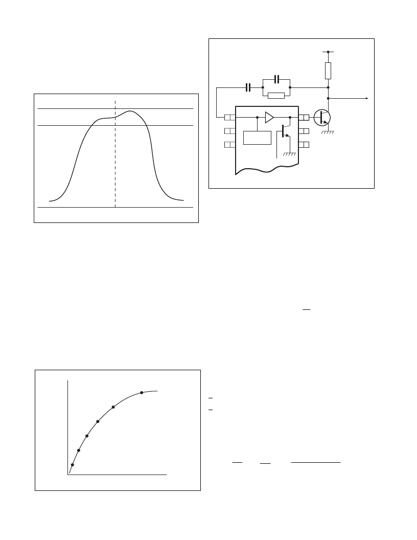
USE OF VARACTOR LINE DISABLE (OS BIT) IN
TUNER ALIGNMENT
In tuner manufacture, many of the wound components
must be aligned to give the desired tilt factors, filter matching
and correcting range for local oscillators and IF output.
This is a time-consuming process and is usually carried out
by tuning the synthesiser to a number of different channels and
aligning to these points (shown
G
on Fig.17).
Each time a new channel is selected, data must first be
written to the synthesiser. In this example, 6 sets of data must
be sent from the micro to the synthesiser.
However, if the varactor line disable bit OS is used, the
varactor line voltage can be externally controlled. This allows
the selected channels to be tuned without the use of a micro to
address and program the device.
The varactor line disable facility is available on all Mitel I
2
C
bus synthesisers and also on I
2
C bus compatible 3-wire
synthesisers such as the SP5024 and SP5054. With the latter
devices, the varactor drive is disabled by applying a negative
voltage to the ENABLE pin (pin 10) and sourcing greater than
350μA from the device. using this method of tuning can result
in appreciable saving of test time.
38.9MHz
Fig.16 Alignment of IF output
Fig.17 Varactor tuning curve
VARACTOR VOLTAGE
C
CHARGE
PUMP
1
2
3
18
17
16
OS
EXTERNAL
ALIGNMENT
VOLTAGE
1
30V
Fig.18 Application of external tuning voltage
相關(guān)PDF資料 |
PDF描述 |
|---|---|
| SP5055 | 2.6GHz Bidirectional IIC BUS Controlled Synthesiser(2.6GHz 雙向IIC總線控制的頻率合成器) |
| SP5070 | 2.4GHz Fixed Modulus Frequency Synthesiser(2.4GHz固定模數(shù)頻率合成器) |
| SP5502 | 1.3GHz IIC Bus 4-Address Synthesiser(1.3GHz IIC總線的頻率合成器(帶4條可編程IIC總線地址)) |
| SP5510 | 1.3GHz Bidirectional IIC Bus Controlled Synthesiser(1.3GHz 雙向IIC總線控制的頻率合成器) |
| SP5512 | 1.3GHz Bidirectional IIC Bus Controlled Synthesiser(1.3GHz 雙向IIC總線控制的頻率合成器) |
相關(guān)代理商/技術(shù)參數(shù) |
參數(shù)描述 |
|---|---|
| SP5055SMP | 制造商:MITEL 制造商全稱:Mitel Networks Corporation 功能描述:2.6GHz Bidirectional I2C BUS Controlled Synthesiser |
| SP505A | 制造商:BLKBOX 功能描述: |
| SP505AB | 制造商:SIPEX 制造商全稱:Sipex Corporation 功能描述:WAN Multi-Mode Serial Transceiver |
| SP505ACF | 制造商: 功能描述: 制造商:Exar Corporation 功能描述: 制造商:undefined 功能描述: |
| SP505ACF-L | 制造商:Exar Corporation 功能描述:TRANSCEIVER MULTI MODE SMD 505 制造商:Exar 功能描述:Transceiver WAN Multi-Mode 10Mbps MQFP80 |
發(fā)布緊急采購(gòu),3分鐘左右您將得到回復(fù)。