- 您現(xiàn)在的位置:買賣IC網(wǎng) > PDF目錄10218 > SP3238ECA-L/TR (Exar Corporation)IC TXRX RS232 INTELLIGENT 28SSOP PDF資料下載

8
Exar Corporation 48720 Kato Road, Fremont CA, 94538 510-668-7017 www.exar.com
SP3238E_100_020111
Receivers
The receivers convert +5.0V EIA/TIA-232
levels to TTL or CMOS logic output levels. Re-
ceivers are High-Z when the AUTO ON-LINE
circuitry is enabled or when in shutdown.
The SP3238E includes an additional non-in-
verting receiver with an output R
1OUT. R1OUT
is an extra output that remains active and
monitors activity while the other receiver
outputs are forced into high impedance.
This allows a Ring Indicator (RI) signal from a
peripheral to be monitored without forward
biasing the TTL/CMOS inputs of the other
devices connected to the receiver outputs.
Since receiver input is usually from a transmis-
sion line where long cable lengths and system
interference can degrade the signal, the inputs
have a typical hysteresis margin of 300mV. This
ensures that the receiver is virtually immune to
noisy transmission lines. Should an input be left
unconnected, an internal 5k pulldown resistor
to ground will commit the output of the receiver
to a HIGH state.
Charge Pump
The charge pump is an Exar–patented design
(U.S. 5,306,954) and uses a unique approach
compared to older less–efficient designs.
The charge pump still requires four external
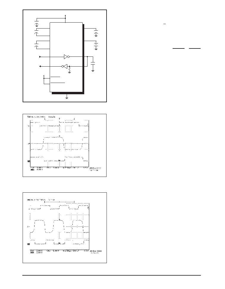
Figure 7. Loopback Test Circuit for RS-232 Driver
Data Transmission Rates
capacitors, but uses a four–phase voltage
shifting technique to attain symmetrical 5.5V
power supplies. The internal power supply
consists of a regulated dual charge pump that
provides output voltages 5.5V regardless of
the input voltage (V
CC) over the +3.0V to +5.5V
range. This is important to maintain compli-
ant RS-232 levels regardless of power supply
fluctuations.
Figure 9. Loopback Test results at 250Kbps
(All Drivers Fully Loaded)
Figure 8. Loopback Test results at 120kbps
(All Drivers Fully Loaded)
SP3238E
TxIN
TxOUT
C1+
C1-
C2+
C2-
V+
V-
VCC
0.1F
+
C2
C5
C1
+
C3
C4
+
LOGIC
INPUTS
VCC
5k
RxIN
RxOUT
LOGIC
OUTPUTS
SHUTDOWN
GND
VCC
ONLINE
1000pF
0.1F
相關(guān)PDF資料 |
PDF描述 |
|---|---|
| SP3243EUCR-L/TR | IC TXRX RS232 INTELLIGENT 32QFN |
| EN3C10F26SX | CONN PLUG 10POS FEMALE CORD #26 |
| EN3C10F26X | CONN PLUG 10POS FEMALE CORD #26 |
| VI-2N0-IW-S | CONVERTER MOD DC/DC 5V 100W |
| AD7824KRZ-REEL | IC ADC 8BIT LC2MOS 4CH HS 24SOIC |
相關(guān)代理商/技術(shù)參數(shù) |
參數(shù)描述 |
|---|---|
| SP3238ECY | 制造商:Rochester Electronics LLC 功能描述: 制造商:Exar Corporation 功能描述: |
| SP3238ECY/TR | 制造商:Rochester Electronics LLC 功能描述: 制造商:Exar Corporation 功能描述: |
| SP3238ECY-L | 功能描述:RS-232接口集成電路 Intel. +3V to +5.5V RS-232 RoHS:否 制造商:Exar 數(shù)據(jù)速率:52 Mbps 工作電源電壓:5 V 電源電流:300 mA 工作溫度范圍:- 40 C to + 85 C 安裝風(fēng)格:SMD/SMT 封裝 / 箱體:LQFP-100 封裝: |
| SP3238ECY-L/TR | 功能描述:RS-232接口集成電路 Intel. +3V to +5.5V RS-232 RoHS:否 制造商:Exar 數(shù)據(jù)速率:52 Mbps 工作電源電壓:5 V 電源電流:300 mA 工作溫度范圍:- 40 C to + 85 C 安裝風(fēng)格:SMD/SMT 封裝 / 箱體:LQFP-100 封裝: |
| SP3238EE | 制造商:SIPEX 制造商全稱:Sipex Corporation 功能描述:Intelligent +3.0V to +5.5V RS-232 Transceiver |
發(fā)布緊急采購,3分鐘左右您將得到回復(fù)。