- 您現(xiàn)在的位置:買賣IC網(wǎng) > PDF目錄225203 > SN54HCT373FKR (TEXAS INSTRUMENTS INC) HCT SERIES, 8-BIT DRIVER, TRUE OUTPUT, CQCC20 PDF資料下載
參數(shù)資料
| 型號(hào): | SN54HCT373FKR |
| 廠商: | TEXAS INSTRUMENTS INC |
| 元件分類: | 總線收發(fā)器 |
| 英文描述: | HCT SERIES, 8-BIT DRIVER, TRUE OUTPUT, CQCC20 |
| 封裝: | CERAMIC, LCC-20 |
| 文件頁數(shù): | 3/6頁 |
| 文件大?。?/td> | 96K |
| 代理商: | SN54HCT373FKR |
SN54HCT373, SN74HCT373
OCTAL TRANSPARENT D-TYPE LATCHES
WITH 3-STATE OUTPUTS
SCLS009B – MARCH 1984 – REVISED MAY 1997
3
POST OFFICE BOX 655303
DALLAS, TEXAS 75265
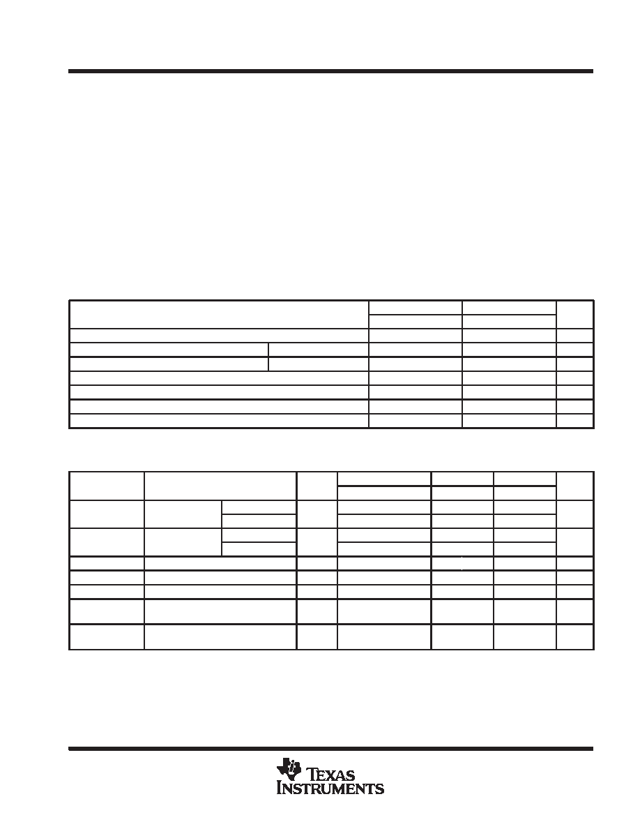
absolute maximum ratings over operating free-air temperature range
Supply voltage range, VCC
–0.5 V to 7 V
. . . . . . . . . . . . . . . . . . . . . . . . . . . . . . . . . . . . . . . . . . . . . . . . . . . . . . . . . .
Input clamp current, IIK (VI < 0 or VI > VCC) (see Note 1)
±20 mA
. . . . . . . . . . . . . . . . . . . . . . . . . . . . . . . . . . . .
Output clamp current, IOK (VO < 0 or VO > VCC) (see Note 1)
±20 mA
. . . . . . . . . . . . . . . . . . . . . . . . . . . . . . . .
Continuous output current, IO (VO = 0 to VCC)
±35 mA
. . . . . . . . . . . . . . . . . . . . . . . . . . . . . . . . . . . . . . . . . . . . . .
Continuous current through VCC or GND
±70 mA
. . . . . . . . . . . . . . . . . . . . . . . . . . . . . . . . . . . . . . . . . . . . . . . . . . .
Package thermal impedance,
θJA (see Note 2): DW package
97
°C/W
. . . . . . . . . . . . . . . . . . . . . . . . . . . . . . . . .
N package
67
°C/W
. . . . . . . . . . . . . . . . . . . . . . . . . . . . . . . . . . .
Storage temperature range, Tstg
–65
°C to 150°C
. . . . . . . . . . . . . . . . . . . . . . . . . . . . . . . . . . . . . . . . . . . . . . . . . . .
Stresses beyond those listed under “absolute maximum ratings” may cause permanent damage to the device. These are stress ratings only, and
functional operation of the device at these or any other conditions beyond those indicated under “recommended operating conditions” is not
implied. Exposure to absolute-maximum-rated conditions for extended periods may affect device reliability.
NOTES:
1. The input and output voltage ratings may be exceeded if the input and output current ratings are observed.
2. The package thermal impedance is calculated in accordance with JESD 51, except for through-hole packages, which use a trace
length of zero.
recommended operating conditions
SN54HCT373
SN74HCT373
UNIT
MIN
NOM
MAX
MIN
NOM
MAX
UNIT
VCC
Supply voltage
4.5
5
5.5
4.5
5
5.5
V
VIH
High-level input voltage
VCC = 4.5 V to 5.5 V
2
V
VIL
Low-level input voltage
VCC = 4.5 V to 5.5 V
0
0.8
0
0.8
V
VI
Input voltage
0
VCC
0
VCC
V
VO
Output voltage
0
VCC
0
VCC
V
tt
Input transition (rise and fall) time
0
500
0
500
ns
TA
Operating free-air temperature
–55
125
–40
85
°C
electrical characteristics over recommended operating free-air temperature range (unless
otherwise noted)
PARAMETER
TEST CONDITIONS
VCC
TA = 25°C
SN54HCT373
SN74HCT373
UNIT
PARAMETER
TEST CONDITIONS
VCC
MIN
TYP
MAX
MIN
MAX
MIN
MAX
UNIT
VOH
VI =VIH or VIL
IOH = –20 A
45 V
4.4
4.499
4.4
V
VOH
VI = VIH or VIL
IOH = –6 mA
4.5 V
3.98
4.3
3.7
3.84
V
VOL
VI =VIH or VIL
IOL = 20 A
45 V
0.001
0.1
V
VOL
VI = VIH or VIL
IOL = 6 mA
4.5 V
0.17
0.26
0.4
0.33
V
II
VI = VCC or 0
5.5 V
±0.1
±100
±1000
nA
IOZ
VO = VCC or 0
5.5 V
±0.01
±0.5
±10
±5
A
ICC
VI = VCC or 0,
IO = 0
5.5 V
8
160
80
A
ICC
One input at 0.5 V or 2.4 V,
Other inputs at 0 or VCC
5.5 V
1.4
2.4
3
2.9
mA
Ci
4.5 V
to 5.5 V
3
10
pF
This is the increase in supply current for each input that is at one of the specified TTL voltage levels rather than 0 V or VCC.
相關(guān)PDF資料 |
PDF描述 |
|---|---|
| SN54LS77J | LS SERIES, DUAL HIGH LEVEL TRIGGERED D LATCH, TRUE OUTPUT, CDIP14 |
| SN54LS90W | DECADE, DIVIDE-BY-TWELVE AND BINARY COUNTERS |
| SN54LS91 | 8-BIT SHIFT REGISTERS |
| SN65ALS172A | Quadruple Differential Line Driver |
| SN74172 | 16-Bit Multiple-Port Register File with 3-State Outputs |
相關(guān)代理商/技術(shù)參數(shù) |
參數(shù)描述 |
|---|---|
| SN54HCT373J | 制造商:Texas Instruments 功能描述:Latch Transparent 3-ST 8-CH D-Type 20-Pin CDIP Tube 制造商:Rochester Electronics LLC 功能描述:- Bulk 制造商:Texas Instruments 功能描述:LATCH TRANSPARENT 3-ST 8CH D-TYPE 20CDIP - Rail/Tube |
| SN54HCT374J | 制造商:Texas Instruments 功能描述:Flip Flop D-Type Bus Interface Pos-Edge 3-ST 1-Element 20-Pin CDIP Tube 制造商:Texas Instruments 功能描述:FLIP FLOP D-TYPE BUS INTRFC POS-EDGE 3-ST 1-ELEM 20CDIP - Rail/Tube |
| SN54HCT541J | 制造商:Texas Instruments 功能描述:Buffer/Line Driver 8-CH Non-Inverting 3-ST CMOS 20-Pin CDIP Tube 制造商:Rochester Electronics LLC 功能描述:- Bulk |
| SN54HCU04J | 制造商:Texas Instruments 功能描述:HEX INVERTER - Rail/Tube 制造商:Texas Instruments 功能描述:Inverter 6-Element CMOS 14-Pin CDIP Tube |
| SN54L00W | 制造商:MAJOR 功能描述: |
發(fā)布緊急采購(gòu),3分鐘左右您將得到回復(fù)。