- 您現(xiàn)在的位置:買賣IC網(wǎng) > PDF目錄374848 > SN54AC08J (Texas Instruments, Inc.) QUADRUPLE 2-INPUT POSITIVE-AND GATES PDF資料下載
參數(shù)資料
| 型號: | SN54AC08J |
| 廠商: | Texas Instruments, Inc. |
| 英文描述: | QUADRUPLE 2-INPUT POSITIVE-AND GATES |
| 中文描述: | 四2輸入陽性與門 |
| 文件頁數(shù): | 1/5頁 |
| 文件大小: | 80K |
| 代理商: | SN54AC08J |
SN54AC08, SN74AC08
QUADRUPLE 2-INPUT POSITIVE-AND GATES
SCAS536B – SEPTEMBER 1995 – REVISED SEPTEMBER 1996
1
POST OFFICE BOX 655303
DALLAS, TEXAS 75265
EPIC
(Enhanced-Performance Implanted
CMOS) 1-
μ
m Process
Package Options Include Plastic
Small-Outline (D), Shrink Small-Outline
(DB), and Thin Shrink Small-Outline (PW)
Packages, Ceramic Chip Carriers (FK) and
Flatpacks (W), and Standard Plastic (N) and
Ceramic (J) DIPS
description
The ’AC08 are quadruple 2-input positive-AND
gates. These devices perform the Boolean
function Y = A B or Y = A + B in positive logic.
The SN54AC08 is characterized for operation
over the full military temperature range of –55
°
C
to 125
°
C. The SN74AC08 is characterized for
operation from –40
°
C to 85
°
C.
FUNCTION TABLE
(each gate)
INPUTS
OUTPUT
Y
A
B
H
H
H
L
X
L
X
L
L
logic symbol
1
1A
2
1B
1Y
3
4
2A
2Y
6
3Y
8
&
5
2B
9
3A
10
3B
12
4A
13
4B
4Y
11
This symbol is in accordance with ANSI/IEEE Std 91-1984 and
IEC Publication 617-12.
Pin numbers shown are for the D, DB, J, N, PW, and W packages.
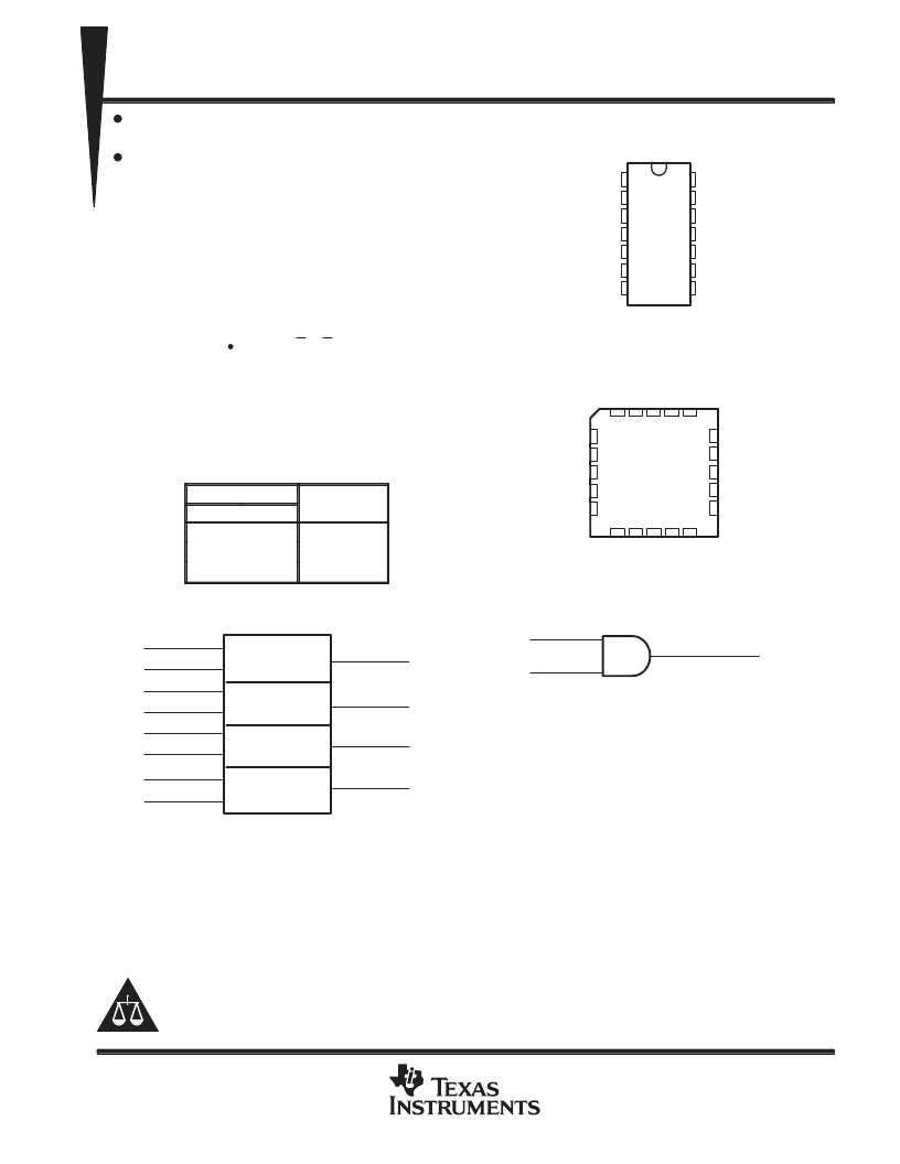
logic diagram, each gate (positive logic)
Y
A
B
Copyright
1996, Texas Instruments Incorporated
PRODUCTION DATA information is current as of publication date.
Products conform to specifications per the terms of Texas Instruments
standard warranty. Production processing does not necessarily include
testing of all parameters.
EPIC is a trademark of Texas Instruments Incorporated.
Please be aware that an important notice concerning availability, standard warranty, and use in critical applications of
Texas Instruments semiconductor products and disclaimers thereto appears at the end of this data sheet.
SN54AC08 . . . J OR W PACKAGE
SN74AC08 . . . D, DB, N, OR PW PACKAGE
(TOP VIEW)
1
2
3
4
5
6
7
14
13
12
11
10
9
8
1A
1B
1Y
2A
2B
2Y
GND
V
CC
4B
4A
4Y
3B
3A
3Y
3
2
1 20 19
9 10 11 12 13
4
5
6
7
8
18
17
16
15
14
4A
NC
4Y
NC
3B
1Y
NC
2A
NC
2B
SN54AC08 . . . FK PACKAGE
(TOP VIEW)
1
1
N
3
3
C
2
G
N
NC – No internal connection
4
相關PDF資料 |
PDF描述 |
|---|---|
| SN54AC08W | QUADRUPLE 2-INPUT POSITIVE-AND GATES |
| SN74AC08DB | QUADRUPLE 2-INPUT POSITIVE-AND GATES |
| SN54AC240FK | OCTAL BUFFERS/DRIVERS WITH 3-STATE OUTPUTS |
| SN54AC240J | OCTAL BUFFERS/DRIVERS WITH 3-STATE OUTPUTS |
| SN54AC240W | OCTAL BUFFERS/DRIVERS WITH 3-STATE OUTPUTS |
相關代理商/技術參數(shù) |
參數(shù)描述 |
|---|---|
| SN54AC08W | 制造商:TI 制造商全稱:Texas Instruments 功能描述:QUADRUPLE 2-INPUT POSITIVE-AND GATES |
| SN54AC10 | 制造商:TI 制造商全稱:Texas Instruments 功能描述:TRIPLE 3-INPUT POSITIVE-NAND GATES |
| SN54AC10FK | 制造商:TI 制造商全稱:Texas Instruments 功能描述:TRIPLE 3-INPUT POSITIVE-NAND GATES |
| SN54AC10J | 制造商:TI 制造商全稱:Texas Instruments 功能描述:TRIPLE 3-INPUT POSITIVE-NAND GATES |
| SN54AC10W | 制造商:TI 制造商全稱:Texas Instruments 功能描述:TRIPLE 3-INPUT POSITIVE-NAND GATES |
發(fā)布緊急采購,3分鐘左右您將得到回復。