- 您現(xiàn)在的位置:買賣IC網(wǎng) > PDF目錄373434 > SN54ABT620A (Texas Instruments, Inc.) Octal Bus Transceivers With 3-State Outputs(八總線收發(fā)器(三態(tài)輸出)) PDF資料下載
參數(shù)資料
| 型號(hào): | SN54ABT620A |
| 廠商: | Texas Instruments, Inc. |
| 英文描述: | Octal Bus Transceivers With 3-State Outputs(八總線收發(fā)器(三態(tài)輸出)) |
| 中文描述: | 八路總線收發(fā)器與三態(tài)輸出(八總線收發(fā)器(三態(tài)輸出)) |
| 文件頁(yè)數(shù): | 1/6頁(yè) |
| 文件大?。?/td> | 129K |
| 代理商: | SN54ABT620A |
SN54ABT620A, SN74ABT620A
OCTAL BUS TRANSCEIVERS
WITH 3-STATE OUTPUTS
SCBS465 – OCTOBER 1992
Copyright
1992, Texas Instruments Incorporated
1
POST OFFICE BOX 655303
DALLAS, TEXAS 75265
State-of-the-Art EPIC-
ΙΙ
B
BiCMOS Design
Significantly Reduces Power Dissipation
ESD Protection Exceeds 2000 V Per
MIL-STD-883C, Method 3015; Exceeds
200 V Using Machine Model (C = 200 pF,
R = 0)
Latch-Up Performance Exceeds 500 mA
Per JEDEC Standard JESD-17
Typical V
OLP
(Output Ground Bounce)
< 1 V at V
CC
= 5 V, T
A
= 25
°
C
High-Drive Outputs (–32-mA I
OH
,
64-mA I
OL
)
Package Options Include Plastic
Small-Outline (DW) and Shrink
Small-Outline (DB) Packages, Ceramic Chip
Carriers (FK), and Standard Plastic and
Ceramic 300-mil DIPs (J, N)
description
The
′
ABT620A bus transceiver is designed for
asynchronous communication between data
buses. The control function implementation allows
for maximum flexibility in timing. The
′
ABT620A
provides inverted data at its outputs.
These devices allow data transmission from the A
bus to the B bus or from the B bus to the A bus
depending upon the logic levels at the
output-enable (OEAB and OEBA) inputs.
The output-enable inputs can be used to disable the device so that the buses are effectively isolated. The
dual-enable configuration gives the transceivers the capability of storing data by simultaneously enabling OEAB
and OEBA. When both OEAB and OEBA are enabled and all other data sources to the two sets of bus lines are
at high impedance, both sets of bus lines (16 in all) will remain at their last states. In this way, each output
reinforces its input in this configuration.
To ensure the high-impedance state during power up or power down, OEBA should be tied to V
CC
through a
pullup resistor; the minimum value of the resistor is determined by the current-sinking capability of the driver.
OEAB should be tied to GND through a pulldown resistor; the minimum value of the resistor is determined by
the current-sourcing capability of the driver.
The SN74ABT620A is packaged in TI’s shrink small-outline package (DB), which provides the same I/O pin
count and functionality of standard small-outline packages in less than half the printed-circuit-board area.
The SN54ABT620A is characterized for operation over the full military temperature range of –55
°
C to 125
°
C.
The SN74ABT620A is characterized for operation from –40
°
C to 85
°
C.
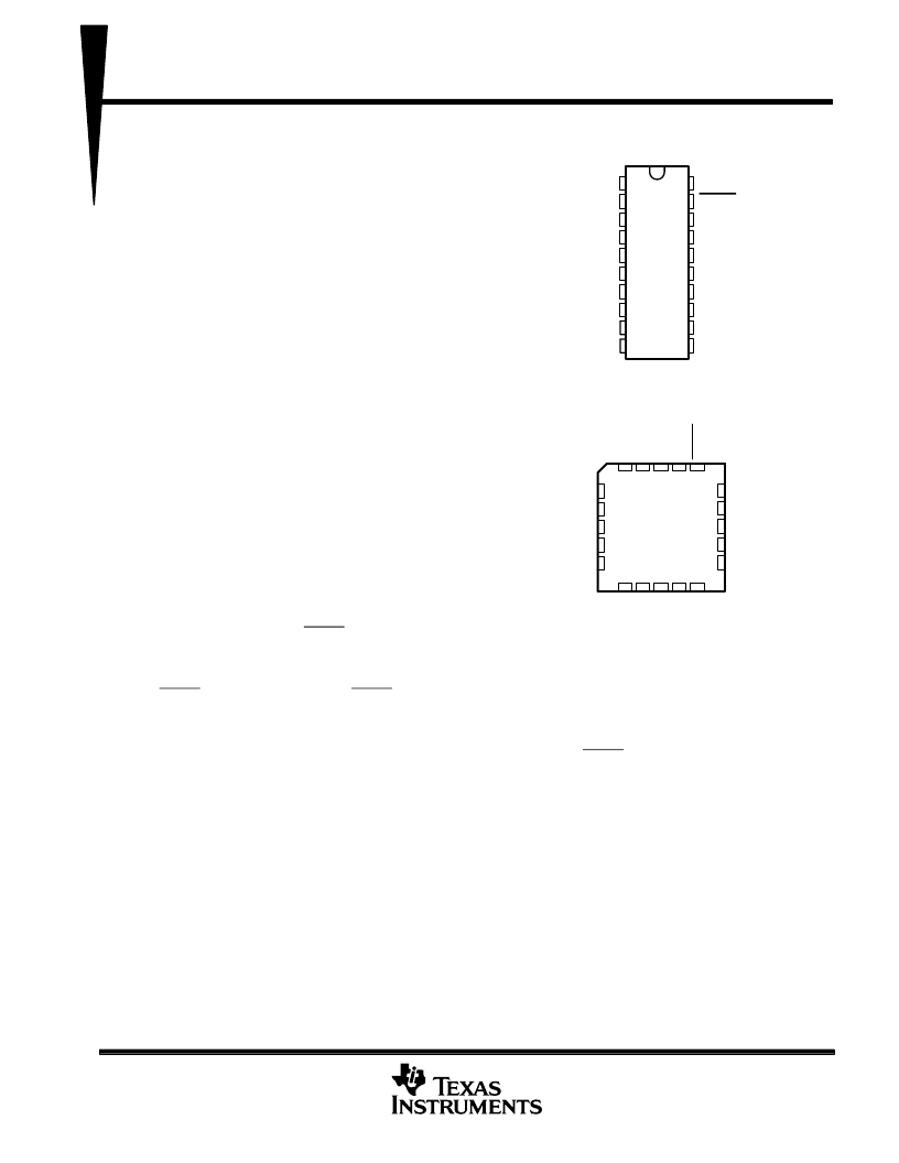
1
2
3
4
5
6
7
8
9
10
20
19
18
17
16
15
14
13
12
11
OEAB
A1
A2
A3
A4
A5
A6
A7
A8
GND
V
CC
OEBA
B1
B2
B3
B4
B5
B6
B7
B8
SN54ABT620A . . . J PACKAGE
SN74ABT620A . . . DB, DW, OR N PACKAGE
(TOP VIEW)
3
2
1 20 19
9 10 11 12 13
4
5
6
7
8
18
17
16
15
14
B1
B2
B3
B4
B5
A3
A4
A5
A6
A7
SN54ABT620A . . . FK PACKAGE
(TOP VIEW)
A
A
O
B
B
O
A
G
B
V
C
EPIC-
ΙΙ
B is a trademark of Texas Instruments Incorporated.
PRODUCT PREVIEW information concerns products in the formative or
design phase of development. Characteristic data and other
specifications are design goals. Texas Instruments reserves the right to
change or discontinue these products without notice.
P
相關(guān)PDF資料 |
PDF描述 |
|---|---|
| SN74ABT620A | Octal Bus Transceivers with 3-State Outputs(八總線收發(fā)器(三態(tài)輸出)) |
| SN54ABT623AFK | OCTAL BUS TRANSCEIVERS WITH 3-STATE OUTPUTS |
| SN74ABT623DB | OCTAL BUS TRANSCEIVERS WITH 3-STATE OUTPUTS |
| SN74ABT623NSR | OCTAL BUS TRANSCEIVERS WITH 3-STATE OUTPUTS |
| SN74ABT623NSRE4 | OCTAL BUS TRANSCEIVERS WITH 3-STATE OUTPUTS |
相關(guān)代理商/技術(shù)參數(shù) |
參數(shù)描述 |
|---|---|
| SN54ABT620FK | 制造商:TI 制造商全稱:Texas Instruments 功能描述:OCTAL BUS TRANSCEIVERS WITH 3-STATE OUTPUTS |
| SN54ABT620J | 制造商:TI 制造商全稱:Texas Instruments 功能描述:OCTAL BUS TRANSCEIVERS WITH 3-STATE OUTPUTS |
| SN54ABT623A | 制造商:TI 制造商全稱:Texas Instruments 功能描述:OCTAL BUS TRANSCEIVERS WITH 3-STATE OUTPUTS |
| SN54ABT623AFK | 制造商:TI 制造商全稱:Texas Instruments 功能描述:OCTAL BUS TRANSCEIVERS WITH 3-STATE OUTPUTS |
| SN54ABT623AJT | 制造商:TI 制造商全稱:Texas Instruments 功能描述:OCTAL BUS TRANSCEIVERS WITH 3-STATE OUTPUTS |
發(fā)布緊急采購(gòu),3分鐘左右您將得到回復(fù)。