- 您現(xiàn)在的位置:買賣IC網(wǎng) > PDF目錄373433 > SN54ABT16863WD (Texas Instruments, Inc.) 18-BIT BUS TRANSCEIVERS WITH 3-STATE OUTPUTS PDF資料下載
參數(shù)資料
| 型號: | SN54ABT16863WD |
| 廠商: | Texas Instruments, Inc. |
| 元件分類: | 通用總線功能 |
| 英文描述: | 18-BIT BUS TRANSCEIVERS WITH 3-STATE OUTPUTS |
| 中文描述: | 18位總線收發(fā)3態(tài)輸出 |
| 文件頁數(shù): | 1/7頁 |
| 文件大?。?/td> | 121K |
| 代理商: | SN54ABT16863WD |
SN54ABT16863, SN74ABT16863
18-BIT BUS TRANSCEIVERS
WITH 3-STATE OUTPUTS
SCBS225C – JUNE 1992 – REVISED MAY 1997
1
POST OFFICE BOX 655303
DALLAS, TEXAS 75265
Members of the Texas Instruments
Widebus
Family
State-of-the-Art EPIC-
ΙΙ
B
BiCMOS Design
Significantly Reduces Power Dissipation
Latch-Up Performance Exceeds 500 mA Per
JEDEC Standard JESD-17
Typical V
OLP
(Output Ground Bounce) < 1 V
at V
CC
= 5 V, T
A
= 25
°
C
High-Impedance State During Power Up
and Power Down
Distributed V
CC
and GND Pin Configuration
Minimizes High-Speed Switching Noise
Flow-Through Architecture Optimizes PCB
Layout
High-Drive Outputs (–32-mA I
OH
, 64-mA I
OL
)
Package Options Include Plastic 300-mil
Shrink Small-Outline (DL) Package and
380-mil Fine-Pitch Ceramic Flat (WD)
Package Using 25-mil Center-to-Center
Spacings
description
The
transceivers
communication between data buses. The
control-function
implementation
external timing requirements.
’ABT16863
are
18-bit
for
noninverting
asynchronous
designed
minimizes
The ’ABT16863 can be used as two 9-bit
transceivers or one 18-bit transceiver. They allow
data transmission from the A bus to the B bus or
from the B bus to the A bus, depending on the logic
level at the output-enable (OEAB or OEBA)
inputs.
When V
CC
is between 0 and 2.1 V, the device is in the high-impedance state during power up or power down.
However, to ensure the high-impedance state above 2.1 V, OE should be tied to V
CC
through a pullup resistor;
the minimum value of the resistor is determined by the current-sinking capability of the driver.
The SN54ABT16863 is characterized for operation over the full military temperature range of –55
°
C to 125
°
C.
The SN74ABT16863 is characterized for operation from –40
°
C to 85
°
C.
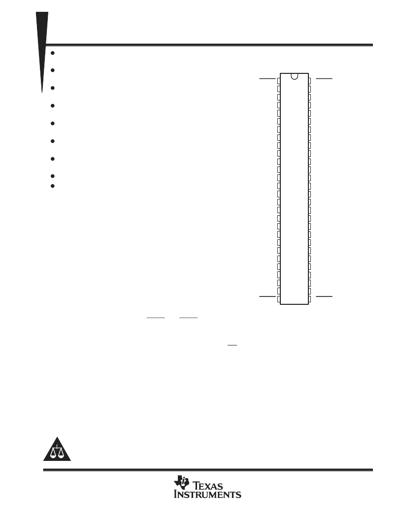
SN54ABT16863 . . . WD PACKAGE
SN74ABT16863 . . . DL PACKAGE
(TOP VIEW)
1
2
3
4
5
6
7
8
9
10
11
12
13
14
15
16
17
18
19
20
21
22
23
24
25
26
27
28
56
55
54
53
52
51
50
49
48
47
46
45
44
43
42
41
40
39
38
37
36
35
34
33
32
31
30
29
1OEAB
1B1
1B2
GND
1B3
1B4
V
CC
1B5
1B6
1B7
GND
1B8
1B9
GND
GND
2B1
2B2
GND
2B3
2B4
2B5
V
CC
2B6
2B7
GND
2B8
2B9
2OEAB
1OEBA
1A1
1A2
GND
1A3
1A4
V
CC
1A5
1A6
1A7
GND
1A8
1A9
GND
GND
2A1
2A2
GND
2A3
2A4
2A5
V
CC
2A6
2A7
GND
2A8
2A9
2OEBA
Copyright
1997, Texas Instruments Incorporated
UNLESS OTHERWISE NOTED this document contains PRODUCTION
DATA information current as of publication date. Products conform to
specifications per the terms of Texas Instruments standard warranty.
parameters.
Widebus and EPIC-
ΙΙ
B are trademarks of Texas Instruments Incorporated.
Please be aware that an important notice concerning availability, standard warranty, and use in critical applications of
Texas Instruments semiconductor products and disclaimers thereto appears at the end of this data sheet.
相關PDF資料 |
PDF描述 |
|---|---|
| SN54ABT16952WD | 16-BIT REGISTERED TRANSCEIVERS WITH 3-STATE OUTPUTS |
| SN74ABT16952DGG | 16-BIT REGISTERED TRANSCEIVERS WITH 3-STATE OUTPUTS |
| SN54ABT16952 | 16-Bit Registered Transceivers With 3-State Outputs(16位記錄收發(fā)器(三態(tài)輸出)) |
| SN54ABT2240AFK | OCTAL BUFFERS AND LINE/MOS DRIVERS WITH 3-STATE OUTPUTS |
| SN54ABT2240AJ | OCTAL BUFFERS AND LINE/MOS DRIVERS WITH 3-STATE OUTPUTS |
相關代理商/技術參數(shù) |
參數(shù)描述 |
|---|---|
| SN54ABT16952 | 制造商:TI 制造商全稱:Texas Instruments 功能描述:16-BIT REGISTERED TRANSCEIVERS WITH 3-STATE OUTPUTS |
| SN54ABT16952_08 | 制造商:TI 制造商全稱:Texas Instruments 功能描述:16-BIT REGISTERED TRANSCEIVERS WITH 3-STATE OUTPUTS |
| SN54ABT16952WD | 制造商:TI 制造商全稱:Texas Instruments 功能描述:16-BIT REGISTERED TRANSCEIVERS WITH 3-STATE OUTPUTS |
| SN54ABT18245 | 制造商:TI 制造商全稱:Texas Instruments 功能描述:SCAN TEST DEVICES WITH 18-BIT BUS TRANSCEIVERS |
| SN54ABT18245A | 制造商:TI 制造商全稱:Texas Instruments 功能描述:SCAN TEST DEVICES WITH 18-BIT BUS TRANSCEIVERS |
發(fā)布緊急采購,3分鐘左右您將得到回復。