- 您現(xiàn)在的位置:買賣IC網(wǎng) > PDF目錄379388 > SM5170AV (Seiko NPC Corporation) TURN TO RELEASE 30MM BLACK PDF資料下載
參數(shù)資料
| 型號: | SM5170AV |
| 廠商: | Seiko NPC Corporation |
| 英文描述: | TURN TO RELEASE 30MM BLACK |
| 中文描述: | PLL合成器集成電路 |
| 文件頁數(shù): | 5/10頁 |
| 文件大小: | 119K |
| 代理商: | SM5170AV |
SM5170AV
NIPPON PRECISION CIRCUITS—5
FUNCTIONAL DESCRIPTION
Frequency Divider Data
The input data should be specified keeping in mind
the V
DD2
supply. The data is input using CLK,
DATA and LE pins into the shift register and latch
which operate from the V
DD2
ply level, however, is not needed and can be ON or
OFF.
supply. The V
DD1
sup-
The control data input uses a 3-line 24-bit serial
interface comprising the clock (CLK), data input
(DATA) and latch enable (LE). The data is input with
the MSB first. The last two bits (23rd + 24th) are
used as the latch select control bits. Data is written to
the shift register on the rising edge of the clock sig-
nal. Accordingly, the data should change state on the
falling edge of the clock signal. Data is transferred
from the shift register to the latch when the latch
enable (LE) signal goes HIGH. Accordingly, the
latch enable signal should be held LOW while data is
being written to the shift register.
The clock and data input signals are both ignored
when the latch enable signal goes HIGH. Also, the
CLK, DATA and LE inputs should be tied LOW
when not setting data.
Input Data Description
Latch select
The last two data bits determine the status of the shift register data latch.
FIN input frequency Divider (N-counter) Structure
The FIN input frequency divider generates a compar-
ator frequency signal (FV), which is input to the
phase comparator, by dividing the VCO signal input
on pin FIN.
The phase comparator is comprised of dual modulus
prescalers, a 5-bit swallow counter and a 12-bit main
counter.
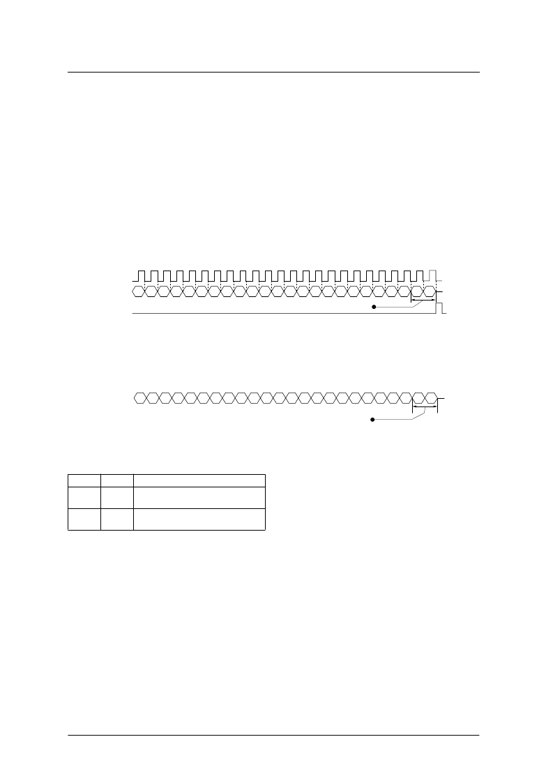
Figure 1. Frequency divider data format
1
2
3
4
5
6
7
8
9
10
11
12
13
14
15
16
17
MSB
CLK
DATA
LE
18
19
20
21
22
23
LSB
Control bits
24
Figure 2. Latch select data format
Bit 23
Bit 24
Latch
0
0
Swallow counter and main counter frequency
divider ratio latch select
0
1
Reference frequency counter divider ratio
data and LD output latch select
1
2
3
4
5
6
7
8
9
10
11
12
13
14
15
16
17
MSB
DATA
18
19
20
21
22
23
LSB
24
Control bits
Frequency settings
Prescaler
Swallow counter
Main counter
FIN input frequency divider ratio
P and P + 1
S
M
N = (P + 1)
N
= P
P = 32, P + 1 = 33
S = 0 to 31
M = 32 to 4095
N = 1056 to 131071
×
S + P
×
(M
S)
×
M + S (where M > S)
Counter set ranges
Prescaler
Swallow counter
Main counter
FIN input frequency divider ratio range
相關PDF資料 |
PDF描述 |
|---|---|
| SM5400 | Surface Mount Si-Rectifiers |
| SM5401 | Surface Mount Si-Rectifiers |
| SM5402 | Surface Mount Si-Rectifiers |
| SM5403 | Surface Mount Si-Rectifiers |
| SM5404 | Surface Mount Si-Rectifiers |
相關代理商/技術參數(shù) |
參數(shù)描述 |
|---|---|
| SM5172 | 制造商:SAMHOP 制造商全稱:SAMHOP 功能描述:3 RF ENCODER |
| SM5172S | 制造商:SAMHOP 制造商全稱:SAMHOP 功能描述:3 RF ENCODER |
| SM517C685KAN480 | 制造商:AVX Corporation 功能描述:- Bulk |
| SM518 | 制造商:Black Box Corporation 功能描述:BLANK PANEL FOR SM500 |
| SM-5180R0FE6 | 功能描述:RES SMD 180 OHM 1% 4W 制造商:vishay dale 系列:SM 包裝:剪切帶(CT) 零件狀態(tài):Digi-Key 停止供應 電阻值:180 Ohms 容差:±1% 功率(W):4W 成分:繞線 特性:- 溫度系數(shù):±20ppm/°C 工作溫度:-55°C ~ 275°C 封裝/外殼:8230 J 形引線 供應商器件封裝:SM-5 大小/尺寸:0.820" 長 x 0.295" 寬(20.83mm x 7.49mm) 高度 - 安裝(最大值):0.305"(7.75mm) 端子數(shù):2 故障率:- 標準包裝:1 |
發(fā)布緊急采購,3分鐘左右您將得到回復。