- 您現(xiàn)在的位置:買賣IC網(wǎng) > PDF目錄379388 > SM5168BAV (Seiko NPC Corporation) PLL Frequency Symthesizer ICs PDF資料下載
參數(shù)資料
| 型號(hào): | SM5168BAV |
| 廠商: | Seiko NPC Corporation |
| 英文描述: | PLL Frequency Symthesizer ICs |
| 中文描述: | 鎖相環(huán)頻率Symthesizer集成電路 |
| 文件頁數(shù): | 2/2頁 |
| 文件大小: | 27K |
| 代理商: | SM5168BAV |
pemnr
SM5168BAV
NIPPON PRECISION CIRCUITS—2
NC9629AE
1998.08
NIPPON PRECISION CIRCUITS INC. reserves the right to make changes to the products described in this data sheet in order to
improve the design or performance and to supply the best possible products. Nippon Precision Circuits Inc. assumes no responsibility for
the use of any circuits shown in this data sheet, conveys no license under any patent or other rights, and makes no claimthat the circuits
are free frompatent infringement. Applications for any devices shown in this data sheet are for illustration only and Nippon Precision
Circuits Inc. makes no claimor warranty that such applications will be suitable for the use specified without further testing or modification.
The products described in this data sheet are not intended to use for the apparatus which influence human lives due to the failure or
malfunction of the products. Customers are requested to comply with applicable laws and regulations in effect now and hereinafter,
including compliance with export controls on the distribution or dissemnation of the products. Customers shall not export, directly or
indirectly, any products without first obtaining required licenses and approvals fromappropriate government agencies.
NIPPON PRECISION CIRCUITS INC.
4-3, 2-chome Fukuzum
Koto-ku, Tokyo 135-8430, Japan
Telephone: 03-3642-6661
Facsimle: 03-3642-6698
NIPPON PRECISION CIRCUITS INC.
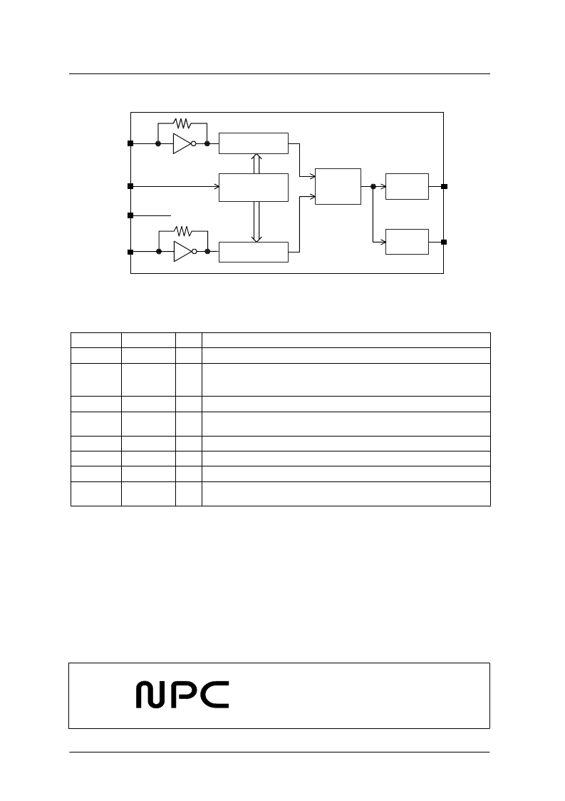
BLOCK DIAGRAM
PIN DESCRIPTION
R-counter
N-counter
Phase
Detector
Charge
Pump
Lock
Detector
LD
DO
FV
DECORDER
XIN
TR
TEST
FIN
Number
Name
I/O
Description
1
VDD
–
2.7 to 3.3V suppply voltage pin.
2
DO
O
PLL phase comparator tristate output pin.
Built-in charge pump means that this output can be connected to a low-pass filter. The output polarity is
preset for connection to a passive filter.
3
VSS
–
Ground pin
4
FIN
I
PLL comparator frequency divider input pin.
Feedback resistor built-in for AC-coupled inputs.
5
TR
I
6
TEST
I
Test pin. should be Open or V
SS
7
LD
O
Unlock signal output pin. Low when unlock.
8
XIN
I
PLL reference frequency divider input pin.
Feedback resistor built-in for AC-coupled inputs.
相關(guān)PDF資料 |
PDF描述 |
|---|---|
| SM5170 | PLL Synthesizer IC |
| SM5170AV | TURN TO RELEASE 30MM BLACK |
| SM5400 | Surface Mount Si-Rectifiers |
| SM5401 | Surface Mount Si-Rectifiers |
| SM5402 | Surface Mount Si-Rectifiers |
相關(guān)代理商/技術(shù)參數(shù) |
參數(shù)描述 |
|---|---|
| SM5168CX | 制造商:NPC 制造商全稱:Nippon Precision Circuits Inc 功能描述:PLL Synthesizer IC |
| SM5168XXV | 制造商:NPC 制造商全稱:Nippon Precision Circuits Inc 功能描述:PLL Synthesizer IC |
| SM516Q | 制造商:DIOTEC 制造商全稱:Diotec Semiconductor 功能描述:Surface Mount Si-Rectifiers |
| SM5170 | 制造商:NPC 制造商全稱:Nippon Precision Circuits Inc 功能描述:PLL Synthesizer IC |
| SM5170AV | 制造商:NPC 制造商全稱:Nippon Precision Circuits Inc 功能描述:PLL Synthesizer IC |
發(fā)布緊急采購,3分鐘左右您將得到回復(fù)。