- 您現(xiàn)在的位置:買賣IC網(wǎng) > PDF目錄48037 > SLD322V-3 830 nm, LASER DIODE PDF資料下載
參數(shù)資料
| 型號(hào): | SLD322V-3 |
| 元件分類: | 激光器 |
| 英文描述: | 830 nm, LASER DIODE |
| 封裝: | M-248 (LO-11), 3 PIN |
| 文件頁(yè)數(shù): | 1/8頁(yè) |
| 文件大?。?/td> | 69K |
| 代理商: | SLD322V-3 |
High Power Density 0.5W Laser Diode
Description
The SLD322V is a high power, gain-guided laser
diode produced by MOCVD method1. Compared to
the SLD300 Series, this laser diode has a high
brightness output with a doubled optical density which
can be achieved by QW-SCH structure2.
1 MOCVD: Metal Organic Chemical Vapor Deposition
2 QW-SCH: Quantum Well Separate Confinement
Heterostructure
Features
High power
Recommended optical power output: Po = 0.5W
Low operating current: Iop = 0.75A (Po = 0.5W)
Applications
Solid state laser excitation
Medical use
Material processes
Measurement
Structure
GaAlAs quantum well structure laser diode
Operating Lifetime
MTTF 10,000H (effective value) at Po = 0.5W, Tc = 25°C
Absolute Maximum Ratings (Tc = 25°C)
Optical power output
Pomax
0.55
W
Reverse voltage
VR
LD
2
V
PD
15
V
Operating temperature (Tc) Topr
–10 to +30
°C
Storage temperature
Tstg
–40 to +85
°C
Warranty
This warranty period shall be 90 days after receipt of the product or 1,000 hours operation time whichever is
shorter.
Sony Quality Assurance Department shall analyze any product that fails during said warranty period, and if the
analysis results show that the product failed due to material or manufacturing defects on the part of Sony, the
product shall be replaced free of charge.
Laser diodes naturally have differing lifetimes which follow a Weibull distribution.
Special warranties are also available.
– 1 –
E93205C19-PS
Sony reserves the right to change products and specifications without prior notice. This information does not convey any license by
any implication or otherwise under any patents or other right. Application circuits shown, if any, are typical examples illustrating the
operation of the devices. Sony cannot assume responsibility for any problems arising out of the use of these circuits.
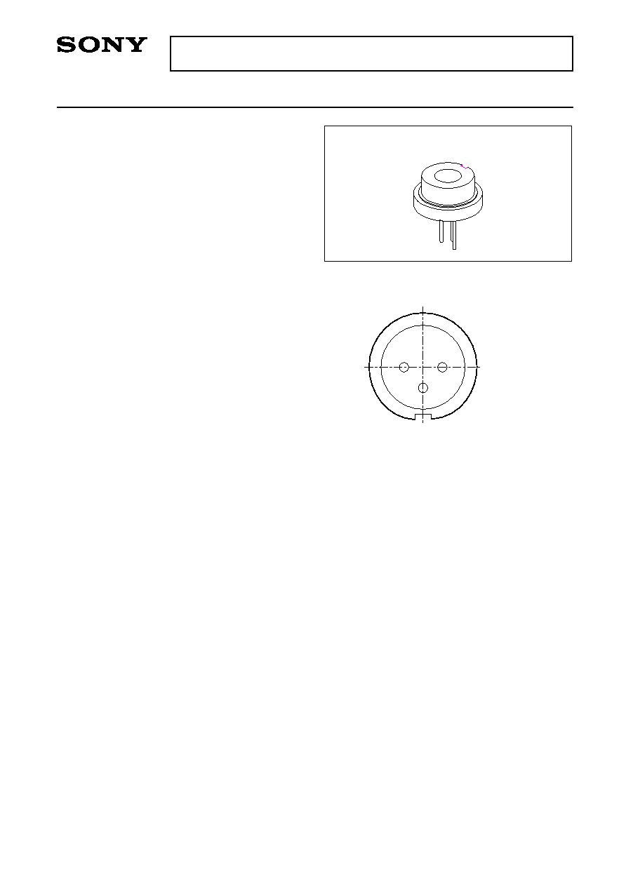
SLD322V
2
Bottom View
1. LD cathode
2. PD anode
3. COMMON
1
3
Pin Configuration
M-248
相關(guān)PDF資料 |
PDF描述 |
|---|---|
| SLD324ZT-25 | 810 nm, LASER DIODE |
| SLD324ZT-21 | 798 nm, LASER DIODE |
| SLD324ZT | 790 nm, LASER DIODE |
| SLDA-61S10-02 | PHOTO DIODE |
| SLDA-61S10-16 | PHOTO DIODE |
相關(guān)代理商/技術(shù)參數(shù) |
參數(shù)描述 |
|---|---|
| SLD322XT | 制造商:SONY 制造商全稱:Sony Corporation 功能描述:0.5W High Power Laser Diode |
| SLD322XT-1 | 制造商:SONY 制造商全稱:Sony Corporation 功能描述:0.5W High Power Laser Diode |
| SLD322XT-2 | 制造商:SONY 制造商全稱:Sony Corporation 功能描述:0.5W High Power Laser Diode |
| SLD322XT-21 | 制造商:SONY 制造商全稱:Sony Corporation 功能描述:0.5W High Power Laser Diode |
| SLD322XT-24 | 制造商:SONY 制造商全稱:Sony Corporation 功能描述:0.5W High Power Laser Diode |
發(fā)布緊急采購(gòu),3分鐘左右您將得到回復(fù)。