- 您現(xiàn)在的位置:買(mǎi)賣(mài)IC網(wǎng) > PDF目錄373403 > SL5020 (AUK Corp) LOW VOLTAGE COMPANDER PDF資料下載
參數(shù)資料
| 型號(hào): | SL5020 |
| 廠(chǎng)商: | AUK Corp |
| 英文描述: | LOW VOLTAGE COMPANDER |
| 中文描述: | 低電壓擴(kuò)展器 |
| 文件頁(yè)數(shù): | 3/8頁(yè) |
| 文件大?。?/td> | 93K |
| 代理商: | SL5020 |
KSI-W006-000
3
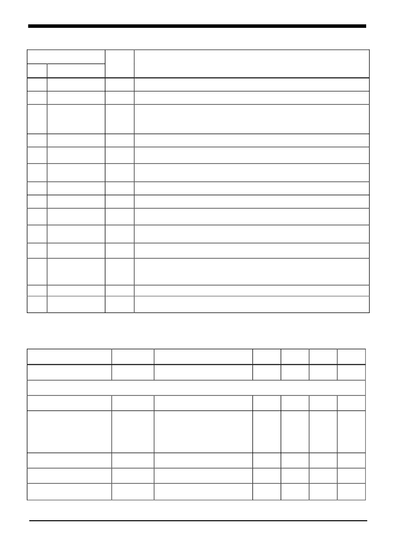
PIN Voltage and Description
Pin
No
Name
Voltage
(V)
Description
1
V
REF
1.3
Bandgap Voltage
2
EXP.MUTE
1.4
Expander mute adjust.
3
EXP.FILTER
0 ~ 0.6
Expander Filter. connect to an external capacitor to filter the full
wave rectifier's output. This capacitor affects attack & delay times, as
well as low frequency accuracy.
4
EXP.OUTPUT
1.5
Output of the expander amplifier
Expander input. Nominally signal range is 3.16mVrms to
316mVrms. Must be capacitor coupled to the signal source
An internal reference voltage. This is an AC ground, and must be
well filtered to obtain high power supply rejection and low crosstalk.
5
EXP.INPUT
1.5
6
VB
2.2
7
GND
GND
Ground
8
COM.FEEDBACK
1.5
Input to the compressor Variable gain stage and rectifier.
Normally, this is connected to the compressor's output through
filtered DC feedback path.
Compressor input, Normally. Signal range is 100uVrms to 1.0Vrms.
Must be capacitor coupled to the signal source
9
COM.CF
1.5
10
COM.INPUT
1.5
11
COM.OUTPUT
1.5
Output of the compressor amplifier.
12
COM.FILTER
0~ 0.6
Compressor filter. Connect to an external capacitor to filter the full
wave rectifier's output. This Capacitor affects attack & decay times,
and low frequency accuracy
Compressor mute adjust.
Power supply pin. Connect to power supply providing between 1.8
and 5.0 V
13
COM.MUTE
1.4
14
Electrical Characteristics
(Unless Otherwise Specified, Ta=25 °C , Vcc=3V, f=1kHz)
Vcc
3
Characteristics
Symbol
Test Conditions
Min.
Typ.
Max.
Unit
Supply current
Icc
No Signal
-
3.1
-
mA
Compressor Section
0 dB Gain
G
C0
Vinc= 100mVrms, 0dB
-1.5
0
1.5
dB
Gain Error
(Note 1)
G
C1
G
C2
G
C3
G
C4
Vinc= 316mVrms, 10dB
Vinc= 10mVrms, -20dB
Vinc= 1mVrms, -40dB
Vinc= 100uVrms, -60dB
-1
-1
-1
-1
0
0
0
0
1
1
1
1
dB
dB
dB
dB
Distortion
THDc
Vinc= 100mVrms, f= 1kHz
0.3
1.5
%
Noise Output
Vnoc
Rg = 600
-
0.8
5.0
mVrms
Ripple Rejection Ratio
RRc
Vcc = 1kHz,
3V(DC), 100mVrms
-
-25
-18
dB
SL5020/P
相關(guān)PDF資料 |
PDF描述 |
|---|---|
| SL5020P | LOW VOLTAGE COMPANDER |
| SL5021 | UNIVERSAL SPEECH NETWORK |
| SL5021P | UNIVERSAL SPEECH NETWORK |
| SL5022 | UNIVERSAL SPEECH NETWORK |
| SL5022P | UNIVERSAL SPEECH NETWORK |
相關(guān)代理商/技術(shù)參數(shù) |
參數(shù)描述 |
|---|---|
| SL5020_1 | 制造商:AUK 制造商全稱(chēng):AUK corp 功能描述:LOW VOLTAGE COMPANDER |
| SL5020P | 制造商:AUK 制造商全稱(chēng):AUK corp 功能描述:LOW VOLTAGE COMPANDER |
| SL5021 | 制造商:AUK 制造商全稱(chēng):AUK corp 功能描述:UNIVERSAL SPEECH NETWORK |
| SL5021P | 制造商:AUK 制造商全稱(chēng):AUK corp 功能描述:UNIVERSAL SPEECH NETWORK |
| SL5022 | 制造商:AUK 制造商全稱(chēng):AUK corp 功能描述:UNIVERSAL SPEECH NETWORK |
發(fā)布緊急采購(gòu),3分鐘左右您將得到回復(fù)。