- 您現在的位置:買賣IC網 > PDF目錄98080 > SI5334C-A00107-GM (SILICON LABORATORIES) PLL BASED CLOCK DRIVER, QCC24 PDF資料下載
參數資料
| 型號: | SI5334C-A00107-GM |
| 廠商: | SILICON LABORATORIES |
| 元件分類: | 時鐘及定時 |
| 英文描述: | PLL BASED CLOCK DRIVER, QCC24 |
| 封裝: | 4 X 4 MM, ROHS COMPLIANT, MO-220VGGD-8, QFN-24 |
| 文件頁數: | 14/34頁 |
| 文件大小: | 233K |
| 代理商: | SI5334C-A00107-GM |
第1頁第2頁第3頁第4頁第5頁第6頁第7頁第8頁第9頁第10頁第11頁第12頁第13頁當前第14頁第15頁第16頁第17頁第18頁第19頁第20頁第21頁第22頁第23頁第24頁第25頁第26頁第27頁第28頁第29頁第30頁第31頁第32頁第33頁第34頁
Si5334
Preliminary Rev. 0.16
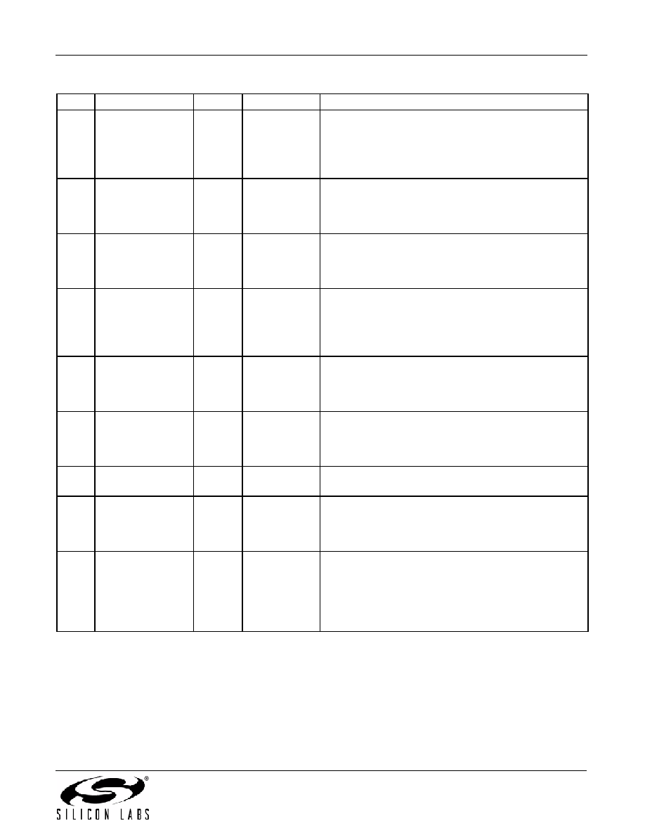
21
17
CLK1B
O
Multi
Output Clock B for Channel 1
May be a single-ended output or half of a differential
output with CLK1A being the other differential half.
If unused, this pin must be tied to VDD pin 24. If unused
leave this pin floating.
18
CLK1A
O
Multi
Output Clock A for Channel 1
May be a single-ended output or half of a differential
output with CLK1B being the other differential half. If
unused leave this pin floating.
19
OEB
I
LVCMOS
Output Enable Low
When low, all the factory-programmed outputs are
enabled. When high all factory programmed outputs are
forced to a logic low.
20
VDDO0
VDD
Supply
Output Clock Supply Voltage.
Supply voltage (3.3, 2.5, 1.8, or 1.5 V) for CLK0A,B.
A 0.1 F capacitor must be located very close to this pin.
If CLK0 is not used, this pin must be tied to VDD (pin 7,
24).
21
CLK0B
O
Multi
Output Clock B for Channel 0
May be a single-ended output or half of a differential
output with CLK0A being the other differential half. If
unused leave this pin floating.
22
CLK0A
O
Multi
Output Clock A for Channel 0
May be a single-ended output or half of a differential
output with CLK0B being the other differential half. If
unused leave this pin floating.
23
RSVD_GND
GND
Ground.
Must be connected to system ground.
24
VDD
Supply
Core Supply Voltage.
The device operates from a 1.8, 2.5, or 3.3 V supply. A
0.1 F bypass capacitor should be located very close to
this pin.
GND
PAD
GND
Ground Pad.
This is the large pad in the center of the package.
Device specifications cannot be guaranteed unless the
ground pad is properly connected to a ground plane on
the PCB. See section 6.0 for the PCB pad sizes and
ground via requirements.
Table 15. Si5334 Pin Descriptions (Continued)
Pin #
Pin Name
I/O
Signal Type
Description
相關PDF資料 |
PDF描述 |
|---|---|
| SI5334C-A00140-GMR | PLL BASED CLOCK DRIVER, QCC24 |
| SI5334B-A00109-GM | PLL BASED CLOCK DRIVER, QCC24 |
| SI5334B-A00121-GMR | PLL BASED CLOCK DRIVER, QCC24 |
| SI5334C-A00115-GM | PLL BASED CLOCK DRIVER, QCC24 |
| SI5334C-A00120-GMR | PLL BASED CLOCK DRIVER, QCC24 |
相關代理商/技術參數 |
參數描述 |
|---|---|
| SI5334C-A00112-GM | 制造商:Silicon Laboratories Inc 功能描述:CLOCK - Rail/Tube |
| SI5334C-A00112-GMR | 制造商:Silicon Laboratories Inc 功能描述:CLOCK - Tape and Reel |
| SI5334C-A00115-GM | 制造商:Silicon Laboratories Inc 功能描述:CLOCK - Rail/Tube |
| SI5334C-A00115-GMR | 制造商:Silicon Laboratories Inc 功能描述:CLOCK - Tape and Reel |
| SI5334C-A00116-GM | 制造商:Silicon Laboratories Inc 功能描述:CLOCK - Rail/Tube |
發(fā)布緊急采購,3分鐘左右您將得到回復。