- 您現(xiàn)在的位置:買賣IC網(wǎng) > PDF目錄373394 > SI3044 (Electronic Theatre Controls, Inc.) 3M 401Q IMPERIAL WETORDRY SHEET PDF資料下載
參數(shù)資料
| 型號(hào): | SI3044 |
| 廠商: | Electronic Theatre Controls, Inc. |
| 英文描述: | 3M 401Q IMPERIAL WETORDRY SHEET |
| 中文描述: | 3.3伏催化裂化/ JATE直接訪問安排 |
| 文件頁數(shù): | 32/54頁 |
| 文件大小: | 1407K |
| 代理商: | SI3044 |
第1頁第2頁第3頁第4頁第5頁第6頁第7頁第8頁第9頁第10頁第11頁第12頁第13頁第14頁第15頁第16頁第17頁第18頁第19頁第20頁第21頁第22頁第23頁第24頁第25頁第26頁第27頁第28頁第29頁第30頁第31頁當(dāng)前第32頁第33頁第34頁第35頁第36頁第37頁第38頁第39頁第40頁第41頁第42頁第43頁第44頁第45頁第46頁第47頁第48頁第49頁第50頁第51頁第52頁第53頁第54頁
Si3035
32
Rev. 1.2
Revision Identification
The Si3035 provides the system designer the ability to
determine the revision of the Si3021 and/or the Si3012.
Register 11 identifies the revision of the Si3021 with 4
bits named REVA. Register 13 identifies the revision of
the Si3012 with 4 bits named REVB. Table 19 shows
the values for the various revisions.
Calibration
The Si3035 initiates an auto-calibration by default
whenever the device goes off-hook or experiences a
loss in line power. Calibration is used to remove any
offsets that may be present in the on-chip A/D converter
which
could
affect
the
Auto-calibration is typically initiated after the DAA DC
termination stabilizes and takes 512/Fs seconds to
complete. Due to the large variation in line conditions
and line card behavior that may be presented to the
DAA, it can be beneficial to use manual calibration in
lieu of auto-calibration. Manual calibration should be
executed as close as possible to 512/Fs seconds before
valid transmit/receive data is expected.
The following steps should be taken to implement
manual calibration:
1. The CALD (auto-calibration disable—Register 17) bit must
be set to 1.
2. The MCAL (manual calibration) bit must be toggled to 1
and then 0 to begin and complete the calibration.
3. The calibration will be completed in 512/Fs seconds.
In-Circuit Testing
The Si3035’s advanced design provides the modem
manufacturer with an increased ability to determine
system functionality during production line tests, as well
as support for end-user diagnostics. Four loopback
modes exist allowing increased coverage of system
components. For three of the test modes, a line-side
power source is needed. While a standard phone line
A/D
dynamic
range.
can be used, the test circuit in Figure 1 on page 4 is
adequate. In addition, an off-hook sequence must be
performed to connect the power source to the line-side
chip.
For the start-up test mode, no line-side power is
necessary and no off-hook sequence is required. The
start-up test mode is enabled by default. When the PDL
bit (Register 6, bit 4) is set (the default case), the line
side is in a power-down mode and the DSP-side is in a
digital loop-back mode. In this mode, data received on
SDI is passed through the internal filters and
transmitted on SDO. This path will introduce
approximately 0.9 dB of attenuation on the SDI signal
received. The group delay of both transmit and receive
filters will exist between SDI and SDO. Clearing the
PDL bit disables this mode and the SDO data is
switched to the receive data from the line side. When
the PDL bit is cleared the FDT bit (Register 12, bit 6) will
become
active,
indicating
communication between the line-side and DSP-side.
This can be used to verify that the ISOcap link is
operational.
The remaining test modes require an off-hook sequence
to operate. The following sequence defines the off-hook
requirement:
1. Power up or reset.
2. Program clock generator to desired sample rate.
3. Enable line-side by clearing PDL bit.
4. Issue off-hook
5. Delay 1548/Fs to allow calibration to occur.
6. Set desired test mode.
The ISOcap digital loopback mode allows the data
pump to provide a digital input test pattern on SDI and
receive that digital test pattern back on SDO. To enable
this mode, set the DL bit of Register 1. In this mode, the
isolation barrier is actually being tested. The digital
stream is delivered across the isolation capacitor, C1 of
Figure 16 on page 15, to the line-side device and
returned across the same barrier. In this mode, the
0.9 dB attenuation and filter group delays also exist.
The analog loopback mode allows an external device to
drive the RX pin of the line-side chip and receive the
signal from the TX pin. This mode allows testing of
external components connecting the RJ-11 jack (TIP
and RING) to the line side of the Si3035. To enable this
mode, set the AL bit of Register 2.
The final testing mode, internal analog loopback, allows
the system to test the basic operation of the
transmit/receive path of the line side and the external
components R4, R18, R21, and C5 of Figure 16 on
page 15. In this test mode, the data pump provides a
the
successful
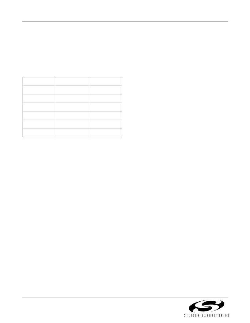
Table 19. Revision Values
Revision
Si3021
Si3012
A
1000
—
B
1001
—
C
1010
—
D
—
0100
E
—
0101
G
—
0111
相關(guān)PDF資料 |
PDF描述 |
|---|---|
| SI3046 | Air Filter; For Use With:Room Air Conditioner ; Height:20"; Peak Reflow Compatible (260 C):No; Thickness:1"; Width:16"; Pack Quantity:1 RoHS Compliant: Yes |
| SI3048 | Air Filter; For Use With:Room Air Conditioner ; Height:25"; Peak Reflow Compatible (260 C):No; Thickness:1"; Width:16"; Pack Quantity:1 RoHS Compliant: Yes |
| SI3014-KS | 3.3 V FCC/JATE DIRECT ACCESS ARRANGEMENT |
| SI3014-KT | 3.3 V FCC/JATE DIRECT ACCESS ARRANGEMENT |
| SI3015-BS | 3.3 V FCC/JATE DIRECT ACCESS ARRANGEMENT |
相關(guān)代理商/技術(shù)參數(shù) |
參數(shù)描述 |
|---|---|
| SI3046 | 制造商:未知廠家 制造商全稱:未知廠家 功能描述:GLOBAL MC 97 SILICON DAA |
| SI3048 | 制造商:未知廠家 制造商全稱:未知廠家 功能描述:GLOBAL MC 97 SILICON DAA |
| SI3050 | 制造商:SILABS 制造商全稱:SILABS 功能描述:Broadband AND Voice Telephony Solutions |
| SI3050C | 制造商:Panasonic Industrial Company 功能描述:IC |
| SI-3050C | 制造商:Allegro MicroSystems 功能描述:Power Supply IC |
發(fā)布緊急采購(gòu),3分鐘左右您將得到回復(fù)。