- 您現(xiàn)在的位置:買賣IC網(wǎng) > PDF目錄373394 > SI3036 (Electronic Theatre Controls, Inc.) Masking Tape; Tape Backing Material:Crepe Paper; Width:24mm; Roll Length:55m; Adhesive Material:Rubber; Color:Natural; Leaded Process Compatible:No; Pack Quantity:1 RoHS Compliant: Yes PDF資料下載
參數(shù)資料
| 型號(hào): | SI3036 |
| 廠商: | Electronic Theatre Controls, Inc. |
| 英文描述: | Masking Tape; Tape Backing Material:Crepe Paper; Width:24mm; Roll Length:55m; Adhesive Material:Rubber; Color:Natural; Leaded Process Compatible:No; Pack Quantity:1 RoHS Compliant: Yes |
| 中文描述: | 3.3伏催化裂化/ JATE直接訪問安排 |
| 文件頁(yè)數(shù): | 18/54頁(yè) |
| 文件大小: | 1407K |
| 代理商: | SI3036 |
第1頁(yè)第2頁(yè)第3頁(yè)第4頁(yè)第5頁(yè)第6頁(yè)第7頁(yè)第8頁(yè)第9頁(yè)第10頁(yè)第11頁(yè)第12頁(yè)第13頁(yè)第14頁(yè)第15頁(yè)第16頁(yè)第17頁(yè)當(dāng)前第18頁(yè)第19頁(yè)第20頁(yè)第21頁(yè)第22頁(yè)第23頁(yè)第24頁(yè)第25頁(yè)第26頁(yè)第27頁(yè)第28頁(yè)第29頁(yè)第30頁(yè)第31頁(yè)第32頁(yè)第33頁(yè)第34頁(yè)第35頁(yè)第36頁(yè)第37頁(yè)第38頁(yè)第39頁(yè)第40頁(yè)第41頁(yè)第42頁(yè)第43頁(yè)第44頁(yè)第45頁(yè)第46頁(yè)第47頁(yè)第48頁(yè)第49頁(yè)第50頁(yè)第51頁(yè)第52頁(yè)第53頁(yè)第54頁(yè)
Si3035
18
Rev. 1.2
Functional Description
The Si3035 is an integrated chipset that provides a
low-cost, isolated, silicon-based interface to the
telephone line. The Si3035 saves cost and board area
by eliminating the need for a modem AFE or serial
codec. It also eliminates the need for an isolation
transformer, relays, opto-isolators, and a 2- to 4-wire
hybrid. The Si3035 solution requires only a few
low-cost,
discrete
components
compliance with FCC Part 68 and JATE out-of-band
noise requirements. See Figure 16 on page 15 for a
typical application circuit. See the pin-compatible
Si3034 or Si3044 data sheets for designs requiring
global support.
The Si3035 North America/Japan DAA offers a number
of new features not supported by the Si3032 device.
These include operation from a single 3.3 V power
supply, JATE (Japan) filter option, finer resolution for
both transmit and receive levels on AOUT (call progress
output), daisy-chaining for up to eight devices, and an
optional IIR filter. Table 15 summarizes the new Si3035
features.
to
achieve
full
Initialization
When the Si3035 is initially powered up, the RESET pin
should be asserted. When the RESET pin is
deasserted, the registers will have default values. This
reset condition guarantees the line-side chip (Si3012) is
powered down with no possibility of loading the line (i.e.,
off-hook). The following is an example initialization
procedure:
1. Program the PLLs with registers 7 to 9 (N1[7:0], M1[7:0],
N2[3:0] and M2[3:0]) to the appropriate divider ratios for
the supplied MCLK frequency and desired sample rate, as
defined in "Clock Generation Subsystem" on page 20.
2. Wait until the PLLs are locked. This time is between
100
μ
S and 1 ms.
3. Write an 0x80 into Register 6. This enables the charge
pump for the V
A
pin, powers up the line-side chip (Si3012),
and enables the AOUT for call progress monitoring.
After this procedure is complete, the Si3035 is ready for
ring detection and off-hook.
Isolation Barrier
The Si3035 achieves an isolation barrier through a
low-cost, high-voltage capacitor in conjunction with
Silicon
Laboratories’
proprietary
processing techniques. These techniques eliminate any
signal degradation due to capacitor mismatches,
common mode interference, or noise coupling. As
shown in Figure 16 on page 15, the C1, C2, and C4
capacitors isolate the Si3021 (DSP-side) from the
Si3012 (line-side). All transmit, receive, control, and
caller ID data are communicated through this barrier.
The ISOcap inter-chip communication is disabled by
default. To enable it, the PDL bit in Register 6 must be
cleared. No communication between the Si3021 and
Si3012 can occur until this bit is cleared. The clock
generator
must
be programmed to an acceptable
sample rate prior to clearing the PDL bit.
Off-Hook
The communication system generates an off-hook
command by applying logic 0 to the OFHK pin or writing
a logic 1 to bit 0 of control Register 5. The OFHK pin
must be enabled by setting bit 1 (OHE) of Register 5.
With OFHK at logic 0, the system is in an off-hook state.
This state is used to seize the line for incoming/outgoing
calls and can also be used for pulse dialing. With OFHK
at logic 1, negligible DC current flows through the
hookswitch. When a logic 0 is applied to the OFHK pin,
the hookswitch transistor pair, Q1 and Q2, turn on. The
net effect of the off-hook signal is the application of a
termination impedance across TIP and RING and the
flow of DC loop current. The termination impedance has
both an AC and a DC component.
The AC termination impedance is a 604-
resistor,
which is connected to the TX pin. The DC termination is
a 51-
resistor, which is connected to the DCT pin.
When executing an off-hook sequence, the Si3035
requires 1548/Fs seconds to complete the off-hook and
provide phone line data on the serial link. This includes
the 12/Fs filter group delay. If necessary, for the shortest
ISOcap
signal
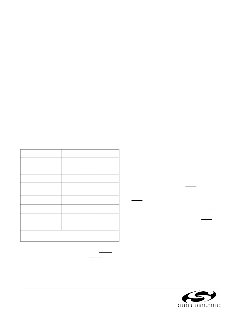
Table 15. New Si3035 Features
Category
Si3032
Si3035
Daisy-Chaining
—
Up to 8 Devices
Optional IIR Filter
—
Yes
Receive Gain
0, 6 dB
0, 3, 6, 9, 12 dB
Transmit Attenuation
0, –3 dB
0, –3, –6 –9,
–12 dB
V
A
5 V
3.3 V* or 5 V
V
D
3.3 V or 5 V
3.3 V or 5 V
JATE Support
—
Yes
AOUT Levels (dB)
0, mute
0, –6, –12, mute
*Note:
The V
A
supply is internally generated by an on-chip
charge pump.
相關(guān)PDF資料 |
PDF描述 |
|---|---|
| SI3038 | Duct Tape; Tape Backing Material:PVC; Width:2"; Roll Length:50yard; Color:Gray; Features:Temperature-stable adhesive, Tears easily and evently by hand, leaves no stciky residue when removed RoHS Compliant: Yes |
| SI3044 | 3M 401Q IMPERIAL WETORDRY SHEET |
| SI3046 | Air Filter; For Use With:Room Air Conditioner ; Height:20"; Peak Reflow Compatible (260 C):No; Thickness:1"; Width:16"; Pack Quantity:1 RoHS Compliant: Yes |
| SI3048 | Air Filter; For Use With:Room Air Conditioner ; Height:25"; Peak Reflow Compatible (260 C):No; Thickness:1"; Width:16"; Pack Quantity:1 RoHS Compliant: Yes |
| SI3014-KS | 3.3 V FCC/JATE DIRECT ACCESS ARRANGEMENT |
相關(guān)代理商/技術(shù)參數(shù) |
參數(shù)描述 |
|---|---|
| SI3038 | 制造商:未知廠家 制造商全稱:未知廠家 功能描述:GLOBAL MC 97 SILICON DAA |
| SI3044 | 制造商:未知廠家 制造商全稱:未知廠家 功能描述:GLOBAL MC 97 SILICON DAA |
| SI3046 | 制造商:未知廠家 制造商全稱:未知廠家 功能描述:GLOBAL MC 97 SILICON DAA |
| SI3048 | 制造商:未知廠家 制造商全稱:未知廠家 功能描述:GLOBAL MC 97 SILICON DAA |
| SI3050 | 制造商:SILABS 制造商全稱:SILABS 功能描述:Broadband AND Voice Telephony Solutions |
發(fā)布緊急采購(gòu),3分鐘左右您將得到回復(fù)。