- 您現(xiàn)在的位置:買賣IC網(wǎng) > PDF目錄373394 > SI3024 (Electronic Theatre Controls, Inc.) GLOBAL MC 97 SILICON DAA PDF資料下載
參數(shù)資料
| 型號: | SI3024 |
| 廠商: | Electronic Theatre Controls, Inc. |
| 英文描述: | GLOBAL MC 97 SILICON DAA |
| 中文描述: | 全球三菱商事97硅DAA |
| 文件頁數(shù): | 23/54頁 |
| 文件大小: | 1407K |
| 代理商: | SI3024 |
第1頁第2頁第3頁第4頁第5頁第6頁第7頁第8頁第9頁第10頁第11頁第12頁第13頁第14頁第15頁第16頁第17頁第18頁第19頁第20頁第21頁第22頁當前第23頁第24頁第25頁第26頁第27頁第28頁第29頁第30頁第31頁第32頁第33頁第34頁第35頁第36頁第37頁第38頁第39頁第40頁第41頁第42頁第43頁第44頁第45頁第46頁第47頁第48頁第49頁第50頁第51頁第52頁第53頁第54頁
Si3035
Rev. 1.2
23
The main design consideration is the generation of a
base frequency, defined as the following:
N1 (Register 7) and M1 (Register 8) are 8-bit unsigned
values. F
MCLK
is the clock provided to the MCLK pin.
Table 18 lists several standard crystal oscillator rates
that could be supplied to MCLK. This list simply
represents a sample of MCLK frequency choices. Many
more are possible.
After the first PLL has been setup, the second PLL can
be programmed easily. The values for N2 and M2
(Register 9) are shown in Table 17. N2 and M2 are 4-bit
unsigned values.
When programming the registers of the clock generator,
the order of register writes is important. For PLL1
updates, N1 (Register 7) must always be written first,
immediately followed by a write to M1 (Register 8). For
PLL2, the CGM bit must be set as desired prior to
writing N2/M2 (Register 9). Changes to the CGM bit
only take effect when N2/M2 are written.
Note:
The values shown in Table 17 and Table 18 satisfy the
equations above. However, when programming the
registers for N1, M1, N2, and M2, the value placed in
these registers must be one less than the value calcu-
lated from the equations. For example, for CGM = 0
with a MCLK of 48.0 MHz, the values placed in the N1
and M1 registers would be 0x7C and 0x5F, respec-
tively. If CGM = 1, a non-zero value must be pro-
grammed to Register 9 in order for the 16/25 ratio to
take effect.
PLL Lock Times
The Si3035 changes sample rates very quickly.
However, lock time will vary based on the programming
of the clock generator. The major factor contributing to
PLL lock time is the CGM bit. When the CGM bit is used
(set to 1), PLL2 will lock slower than when CGM is 0.
The following relationships describe the boundaries on
PLL locking time:
PLL1 lock time < 1 ms (CGM = 0,1)
PLL2 lock time: 100 us to 1 ms (CGM = 0)
PLL2 lock time <1 ms (CGM = 1)
For modem designs, it is recommended that PLL1 be
programmed
during
initialization.
programming of PLL1 is necessary. The CGM bit and
PLL2 can be programmed for the desired initial sample
No
further
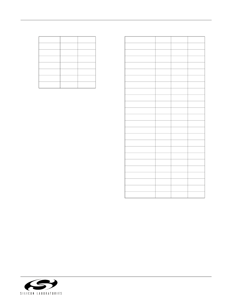
Table 17. N2, M2 Values (CGM = 0, 1)
Fs (Hz)
N2
M2
7200
2
2
8000
9
10
8229
7
8
8400
6
7
9000
4
5
9600
3
4
10286
7
10
FBase
FMCLK
M1
N1
36.864MHz CGM
,
0
=
=
=
FBase
N1 25
16
FMCLKM1
36.864MHz CGM
,
1
=
=
=
Table 18. MCLK Examples
MCLK (MHz)
N1
M1
CGM
1.8432
1
20
0
4.0000
5
72
1
4.0960
1
9
0
5.0688
11
80
0
6.0000
5
48
1
6.1440
1
6
0
8.1920
32
225
1
9.2160
1
4
0
10.0000
25
144
1
10.3680
9
32
0
11.0592
3
10
0
12.288
1
3
0
14.7456
2
5
0
16.0000
5
18
1
18.4320
1
2
0
24.5760
32
75
1
25.8048
7
10
0
33.8688
147
160
0
44.2368
96
125
1
46.0800
5
4
0
47.9232
13
10
0
48.0000
125
96
0
56.0000
35
36
1
60.0000
25
24
1
相關PDF資料 |
PDF描述 |
|---|---|
| SI3014 | GLOBAL MC 97 SILICON DAA |
| SI3025 | COOLER FOR TO-3 20 WATTS |
| Si3200-BS | DUAL PROGRAMMABLE CMOS SLIC WITH LINE MONITORING |
| Si3232 | DUAL PROGRAMMABLE CMOS SLIC WITH LINE MONITORING |
| Si3200-KS | DUAL PROGRAMMABLE CMOS SLIC WITH LINE MONITORING |
相關代理商/技術參數(shù) |
參數(shù)描述 |
|---|---|
| SI3024-KS | 制造商:未知廠家 制造商全稱:未知廠家 功能描述:GLOBAL MC 97 SILICON DAA |
| SI3024-KT | 制造商:未知廠家 制造商全稱:未知廠家 功能描述:GLOBAL MC 97 SILICON DAA |
| SI3025 | 制造商:ALLEGRO 制造商全稱:Allegro MicroSystems 功能描述:LOW-VOLTAGE, HIGH-CURRENT 1.8 V LINEAR REGULATOR |
| SI-3025B | 制造商:SANKEN 制造商全稱:Sanken electric 功能描述:5-Terminal, Multi-Function, Full-Mold, Low Dropout Voltage Dropper Type |
| SI-3025F | 制造商:SANKEN 制造商全稱:Sanken electric 功能描述:5-Terminal, Multi-Function, Full-Mold, Low Dropout Voltage Dropper Type |
發(fā)布緊急采購,3分鐘左右您將得到回復。