- 您現(xiàn)在的位置:買賣IC網(wǎng) > PDF目錄10906 > SI2439-A-GM (Silicon Laboratories Inc)IC ISOMODEM 33.6KBPS 38-QFN PDF資料下載
參數(shù)資料
| 型號: | SI2439-A-GM |
| 廠商: | Silicon Laboratories Inc |
| 文件頁數(shù): | 70/70頁 |
| 文件大小: | 0K |
| 描述: | IC ISOMODEM 33.6KBPS 38-QFN |
| 標準包裝: | 364 |
| 系列: | * |
第1頁第2頁第3頁第4頁第5頁第6頁第7頁第8頁第9頁第10頁第11頁第12頁第13頁第14頁第15頁第16頁第17頁第18頁第19頁第20頁第21頁第22頁第23頁第24頁第25頁第26頁第27頁第28頁第29頁第30頁第31頁第32頁第33頁第34頁第35頁第36頁第37頁第38頁第39頁第40頁第41頁第42頁第43頁第44頁第45頁第46頁第47頁第48頁第49頁第50頁第51頁第52頁第53頁第54頁第55頁第56頁第57頁第58頁第59頁第60頁第61頁第62頁第63頁第64頁第65頁第66頁第67頁第68頁第69頁當前第70頁
Si2494/39
Rev. 1.0
9
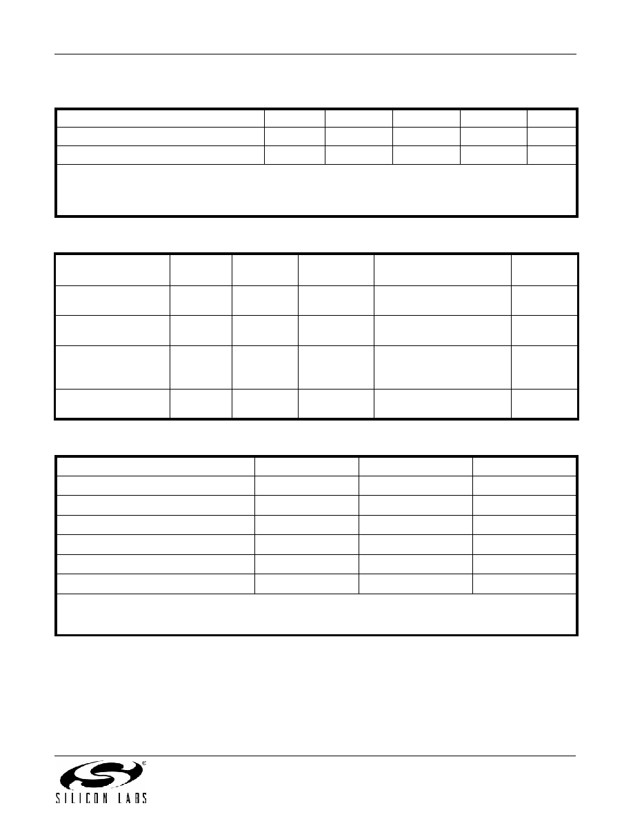
SCLK cycle time
tSCK
224
—
ns
Inactive time between SS actives
tNSS_INACT
81
—
—ns
Table 6. Thermal Conditions
Parameter
Symbol
Test
Condition
Min
Typ
Max
Unit
Thermal Resistance
(Si2494/39)
JA
QFN-38
—
35
—
°C/W
Thermal Resistance
(Si3018)
JA
SOIC-16
—
77
—
°C/W
Maximum Junction
Temperature
(Si2494/39)
T
QFN-38
—
105
°C
Maximum Junction
Temperature (Si3018)
T
SOIC-16
—
110
°C
Table 7. Absolute Maximum Ratings
Parameter
Symbol
Value
Unit
DC Supply Voltage
VD
4.1
V
Input Current, Si2494/39 Digital Input Pins
IIN
±10
mA
Digital Input Voltage
VIND
–0.3 to (VD + 0.3)
V
CLKIN/XTALI Input Voltage
VXIND
–0.3 to (VD + 0.3)
V
Operating Temperature Range
TA
–10 to 100
°C
Storage Temperature Range
TSTG
–40 to 150
°C
Note:
Permanent device damage may occur if the above absolute maximum ratings are exceeded. Functional operation
should be restricted to the conditions as specified in the operational sections of this data sheet. Exposure to absolute
maximum rating conditions for extended periods may affect device reliability.
Table 5. Switching Characteristics1 (Continued)
(VD = 3.0 to 3.6 V, TA = 0 to 70 °C for F-grade, TA = –40 to 85 °C for G-grade)
Parameter
Symbol
Min
Typ
Max
Unit
Notes:
1.
All timing is referenced to the 50% level of the waveform. Input test levels are VIH =VD – 0.4 V, VIL =0.4 V.
2.
With 32.768 kHz clocking, allow 500 to the reset low-to-high minimum pulse on power-up and wake-from-power-down
conditions.
相關(guān)PDF資料 |
PDF描述 |
|---|---|
| PIC16LC72A-04/SS | IC MCU OTP 2KX14 A/D PWM 28SSOP |
| PIC16C72A/JW | IC MCU OTP 2KX14 A/D PWM 28CDIP |
| PIC16C65B/JW | IC MCU EPROM 4KX14 PWM 40CDIP |
| SI2439-A-FM | IC ISOMODEM 33.6KBPS 38-QFN |
| PIC16C62B/JW | IC MCU EPROM 2KX14 PWM 28CDIP |
相關(guān)代理商/技術(shù)參數(shù) |
參數(shù)描述 |
|---|---|
| SI2439-A-GMR | 制造商:Silicon Laboratories Inc 功能描述:33.6 KBPS ISOMODEM + VOICE - Tape and Reel 制造商:Silicon Laboratories Inc 功能描述:IC ISOMODEM 33.6KBPS 38-QFN |
| SI2456 | 制造商:SILABS 制造商全稱:SILABS 功能描述:V.90, V.34, V.32BIS ISOMODEM⑩ WITH INTEGRATED GLOBAL DAA |
| SI2456-FT | 制造商:Silicon Laboratories Inc 功能描述:MODEM CHIP CHIPSET ISOMODEM 56KBPS 24TSSOP - Rail/Tube |
| SI2456-FT/REV F | 制造商:Silicon Laboratories Inc 功能描述:NOT RECOMMENDED FOR NEW DESIGNS, SEE SI2457-FT - Rail/Tube |
| Si2456-FTR | 制造商:Silicon Laboratories Inc 功能描述:MODEM CHIP CHIPSET ISOMODEM 56KBPS 24TSSOP - Tape and Reel |
發(fā)布緊急采購,3分鐘左右您將得到回復。