- 您現(xiàn)在的位置:買賣IC網(wǎng) > PDF目錄374781 > SG3525ADWR2G (ON SEMICONDUCTOR) Pulse Width Modulator Control Circuit PDF資料下載
參數(shù)資料
| 型號(hào): | SG3525ADWR2G |
| 廠商: | ON SEMICONDUCTOR |
| 元件分類: | 穩(wěn)壓器 |
| 英文描述: | Pulse Width Modulator Control Circuit |
| 中文描述: | 0.5 A SWITCHING CONTROLLER, 400 kHz SWITCHING FREQ-MAX, PDSO16 |
| 封裝: | PLASTIC, LEAD FREE, SOIC-16 |
| 文件頁(yè)數(shù): | 1/10頁(yè) |
| 文件大?。?/td> | 155K |
| 代理商: | SG3525ADWR2G |
Semiconductor Components Industries, LLC, 2005
January, 2005 Rev. 5
1
Publication Order Number:
SG3525A/D
SG3525A
Pulse Width Modulator
Control Circuit
The SG3525A pulse width modulator control circuit offers
improved performance and lower external parts count when
implemented for controlling all types of switching power supplies.
The onchip +5.1 V reference is trimmed to
amplifier has an input commonmode voltage range that includes the
reference voltage, thus eliminating the need for external divider
resistors. A sync input to the oscillator enables multiple units to be
slaved or a single unit to be synchronized to an external system clock.
A wide range of deadtime can be programmed by a single resistor
connected between the C
T
and Discharge pins. This device also
features builtin softstart circuitry, requiring only an external timing
capacitor. A shutdown pin controls both the softstart circuitry and the
output stages, providing instantaneous turn off through the PWM latch
with pulsed shutdown, as well as softstart recycle with longer
shutdown commands. The under voltage lockout inhibits the outputs
and the changing of the softstart capacitor when V
CC
is below
nominal. The output stages are totempole design capable of sinking
and sourcing in excess of 200 mA. The output stage of the SG3525A
features NOR logic resulting in a low output for an offstate.
1% and the error
Features
8.0 V to 35 V Operation
5.1 V
1.0% Trimmed Reference
100 Hz to 400 kHz Oscillator Range
Separate Oscillator Sync Pin
Adjustable Deadtime Control
Input Undervoltage Lockout
Latching PWM to Prevent Multiple Pulses
PulsebyPulse Shutdown
Dual Source/Sink Outputs:
PbFree Packages are Available*
400 mA Peak
*For additional information on our PbFree strategy and soldering details, please
download the ON Semiconductor Soldering and Mounting Techniques
Reference Manual, SOLDERRM/D.
MARKING
DIAGRAMS
A
WL = Wafer Lot
YY
= Year
WW = Work Week
= Assembly Location
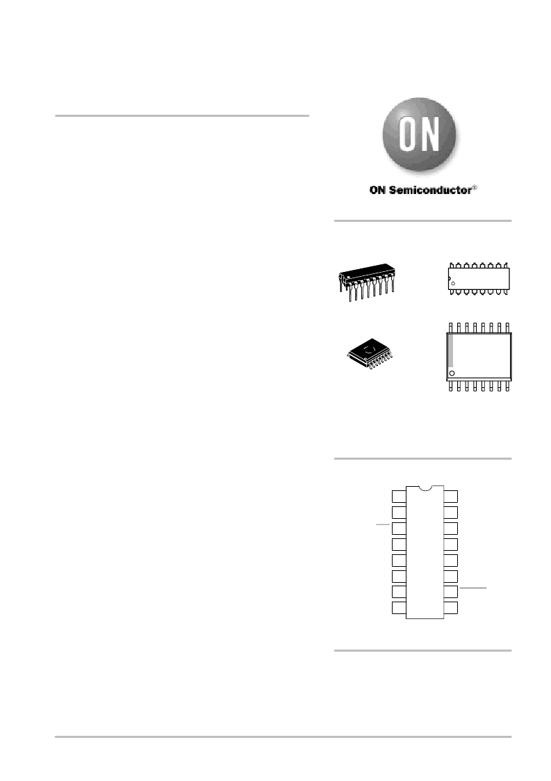
1
16
PDIP16
N SUFFIX
CASE 648
1
16
SG3525AN
AWLYYWW
PIN CONNECTIONS
1
2
3
4
5
6
7
8
9
10
11
12
13
14
15
16
(Top View)
Inv. Input
Sync
OSC. Output
R
T
Discharge
SoftStart
Noninv. Input
C
T
Compensation
Shutdown
Output A
V
C
Output B
V
CC
V
ref
Ground
1
16
SG3525A
AWLYYWW
SOIC16L
DW SUFFIX
CASE 751G
See detailed ordering and shipping information in the package
dimensions section on page 2 of this data sheet.
ORDERING INFORMATION
16
1
http://onsemi.com
相關(guān)PDF資料 |
PDF描述 |
|---|---|
| SG3525ANG | Pulse Width Modulator Control Circuit |
| SG3525A | Pulse Width Modulator Control Circuit(脈寬調(diào)制器控制電路) |
| SG3526 | PULSE WIDTH MODULATION CONTROL CIRCUIT |
| SG3526 | PULSE WIDTH MODULATION CONTROL CIRCUIT |
| SG3526N | PULSE WIDTH MODULATION CONTROL CIRCUIT |
相關(guān)代理商/技術(shù)參數(shù) |
參數(shù)描述 |
|---|---|
| SG3525ADWR2G-CUT TAPE | 制造商:ON 功能描述:SC Series 20 mA 400 kHz Surface Mount PWM Control Circuit - SOIC-16L |
| SG3525AJ | 制造商:Microsemi Corporation 功能描述:SG3525AJ - Bulk |
| SG3525AN | 功能描述:電壓模式 PWM 控制器 Voltage Mode w/Sync RoHS:否 制造商:Texas Instruments 輸出端數(shù)量:1 拓?fù)浣Y(jié)構(gòu):Buck 輸出電壓:34 V 輸出電流: 開(kāi)關(guān)頻率: 工作電源電壓:4.5 V to 5.5 V 電源電流:600 uA 最大工作溫度:+ 125 C 最小工作溫度:- 40 C 封裝 / 箱體:WSON-8 封裝:Reel |
| SG3525AN | 制造商:STMicroelectronics 功能描述:IC PWM CONTROLLER 3525 DIP16 |
| SG3525AN | 制造商:STMicroelectronics 功能描述:IC POWER SUPPLY 35V |
發(fā)布緊急采購(gòu),3分鐘左右您將得到回復(fù)。