- 您現(xiàn)在的位置:買賣IC網(wǎng) > PDF目錄385842 > SG29125 (Microsemi Corporation) LOW DROPOUT DUAL REGULATOR PDF資料下載
參數(shù)資料
| 型號: | SG29125 |
| 廠商: | Microsemi Corporation |
| 英文描述: | LOW DROPOUT DUAL REGULATOR |
| 中文描述: | 低壓差型雙調(diào)節(jié)器 |
| 文件頁數(shù): | 4/4頁 |
| 文件大小: | 41K |
| 代理商: | SG29125 |
SG29125/125A
12/90 Rev 1.1 2/94
Copyright
1994
L
IN
F
IN
ITY
Microelectronics Inc.
11861 Western Avenue
∞
∞
Garden Grove, CA 92841
(714) 898-8121
∞
FAX: (714) 893-2570
4
5-PIN TO-220 PLASTIC
P - PACKAGE
Ambient
Temperature Range
SG29125P
SG29125AP
-40
°
C to 85
°
C
-40
°
C to 85
°
C
Part No.
Package
Connection Diagram
5
4
3
2
1
STANBY OUTPUT
ON/OFF SWITCH
GROUND
OUTPUT VOLTAGE (V
OUT
)
INPUT VOLTAGE (V
IN
)
GND
CONNECTION DIAGRAM & ORDERING INFORMATION
(See Note Below)
APPLICATION HINTS
EXTERNAL CAPACITORS
To stabilize the outputs and prevent oscillation (perhaps by many
volts) external capacitors are required. The minimum recom-
mended value for the output capacitors is 10μF, although the
actual size and type will likely vary according to the particular
application, e.g., operating temperature range and load. Another
consideration is the effective series resistance (ESR) of the
capacitor. Capacitor ESR will vary by manufacturer. Conse-
quently, some evaluation may be required to determine the
minimum value of the output capacitors. Generally worst case
occurs at the maximum load and minimum ambient temperature.
The size of the output capacitor can be increased to any value
above the minimum. One possible advantage of this would be to
maintain the output voltage during brief periods of negative input
transients
The output capacitors chosen should be rated for the full range
of ambient temperature over which the circuit will be exposed and
expected to operate. For example, many aluminum type electro-
lytic capacitors will freeze at -30°C. The effective capacitance is
reduced to zero in such a situation. Capacitors rated for -40°C
operation must be used in order to maintain regulator stability at
that temperature. Tantalum capacitors satisfy this requirement.
STANDBY OUTPUT
The SG29125/125A differs from most fixed voltage regulators in
that it is equipped with two regulator outputs instead of one. The
additional output is intended for use in systems requiring standby
memory circuits. While the high current regulator output can be
controlled with the ON/OFF pin described below, the standby
remains on under all conditions as long as sufficient input voltage
is applied to the IC. Thus, memory and other circuits powered by
this output remain unaffected by positive line transients, thermal
shutdown, etc.
The standby regulator circuit is designed so that the quiescent
current to the IC is very low (<1.5mA) when the other regulator
output is off.
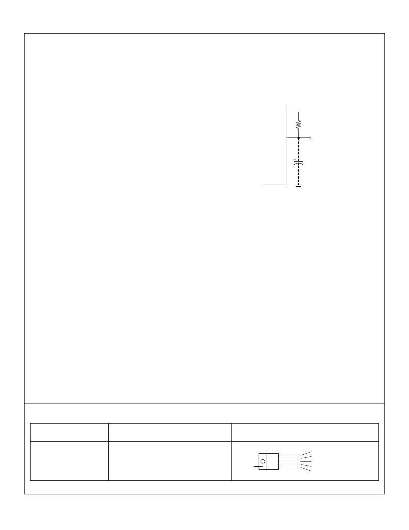
If the standby output is not required it can be disabled. This is
accomplished by connecting a resistor from the standby output to
the supply voltage, thereby also eliminating the requirement for
a more expensive output capacitor to prevent unwanted oscilla-
tions. The resistor value depends upon the minimum input
voltage expected for a given system.
Since the standby output is shunted with an internal 5.6V zener,
the current through the external resistor should be sufficient to
bias internal resistors up to this point. Approximately 60
μ
A will
suffice, resulting in a 10k external resistor for most applications
(Figure 1).
HIGH CURRENT OUTPUT
STANDBY
OUTPUT
V
IN
R
D
10K
C3
FIGURE 1. Disabling Standby Output to Eliminate C3
SG29125/125A
Note: 1. All parts are viewed from the top.
The high current regulated output features fault protection
against overvoltage as well as a thermal shutdown feature. If the
input voltage rises above 33V (load dump), the high current
output shuts down automatically. The internal circuitry is thus
protected and the IC is able to survive higher voltage transients
than might otherwise be expected. The thermal shutdown of the
high current output effectively guards against overheating of the
die since this section of the IC is the principle source of power
dissipation on the chip.
ON/OFF SWITCH
The ON/OFF pin is a high impedance low current switch that
controls the main output voltage (pin 2). This is directly compat-
ible with all 5 volt logic families. For use with open collector logic
outputs, a 100K resistor from this pin to a 5V supply, such as Pin
5, is required.
相關(guān)PDF資料 |
PDF描述 |
|---|---|
| SG29125A | LOW DROPOUT DUAL REGULATOR |
| SG29125AP | LOW DROPOUT DUAL REGULATOR |
| SG29125P | LOW DROPOUT DUAL REGULATOR |
| SG3524N | REGULATING PULSE WIDTH MODULATORS |
| SG3524P | REGULATING PULSE WIDTH MODULATORS |
相關(guān)代理商/技術(shù)參數(shù) |
參數(shù)描述 |
|---|---|
| SG29125_1 | 制造商:MICROSEMI 制造商全稱:Microsemi Corporation 功能描述:LOW DROPOUT DUAL REGULATOR |
| SG29125A | 制造商:MICROSEMI 制造商全稱:Microsemi Corporation 功能描述:LOW DROPOUT DUAL REGULATOR |
| SG29125AP | 制造商:Microsemi Corporation 功能描述:SG29125AP - Bulk |
| SG29125P | 制造商:Microsemi Corporation 功能描述:SG29125P - Bulk |
| SG293037DS | 功能描述:EMI 連接器墊圈 37 Pin D-Sub Shield RoHS:否 制造商:FerriShield 連接器類型: 外殼大小: 厚度:6.35 mm 等級: |
發(fā)布緊急采購,3分鐘左右您將得到回復(fù)。