- 您現(xiàn)在的位置:買賣IC網(wǎng) > PDF目錄66215 > SFH6318T (VISHAY INTERTECHNOLOGY INC) 1 CHANNEL LOGIC OUTPUT OPTOCOUPLER PDF資料下載
參數(shù)資料
| 型號: | SFH6318T |
| 廠商: | VISHAY INTERTECHNOLOGY INC |
| 元件分類: | 光電耦合器 |
| 英文描述: | 1 CHANNEL LOGIC OUTPUT OPTOCOUPLER |
| 封裝: | SOIC-8 |
| 文件頁數(shù): | 1/3頁 |
| 文件大小: | 385K |
| 代理商: | SFH6318T |
Document Number: 83678
www.vishay.com
Revision 17-August-01
2–282
Maximum Ratings (TA=25°C)
Emitter
Reverse Input Voltage ...................................................................3.0 V
Supply and Output Voltage, VCC (pin 8-5), VO (pin 6-5)
SFH6318T ...................................................................... –0.5 to 7.0 V
SFH6319T ....................................................................... –0.5 to 18 V
Input Power Dissipation..............................................................35 mW
Derate Linearly above ............................................................... 50
°C
Free Air Temperature ........................................................0.7 mW/
°C
Average Input Current ................................................................ 20 mA
Peak Input Current ..................................................................... 40 mA
(50% Duty Cycle-1.0 ms pulse width)
Peak Transient Input Current
(tp≤1.0 s, 300 pps).................................................................. 1.0 A
Detector (Si Photodiode + Photodarlington)
Output Current IO (pin 6)............................................................ 60 mA
Emitter-base Reverse Voltage (pin 5-7).........................................0.5 V
Output Power Dissipation.........................................................150 mW
Derate Linearly from 25
°C ................................................2.0 mW/°C
Package
Storage Temperature ..................................................–55
°C to +125°C
Operating Temperature ................................................–40
°C to +85°C
Lead Soldering Temperature (t=10 s) ......................................... 260
°C
Junction Temperature .................................................................. 100
°C
Ambient Temperature Range .....................................–55
°C to +100°C
Isolation Test Voltage between
Emitter and Detector........................................................ 3000 VRMS
(refer to climate DIN 40046, part 2, Nov. 74)
Pollution Degree (DIN VDE 0110) ....................................................... 2
Creepage Distance ................................................................
≥4.0 mm
Clearance ...............................................................................
≥4.0 mm
Comparative Tracking Index
per DIN IEC 112/VDE 0303, part 1 .............................................. 175
Isolation Resistance
VIO=500 V, TA=25°C RISOL................................................... ≥10
12
VIO=500 V, TA=100°C RISOL................................................. ≥10
11
40
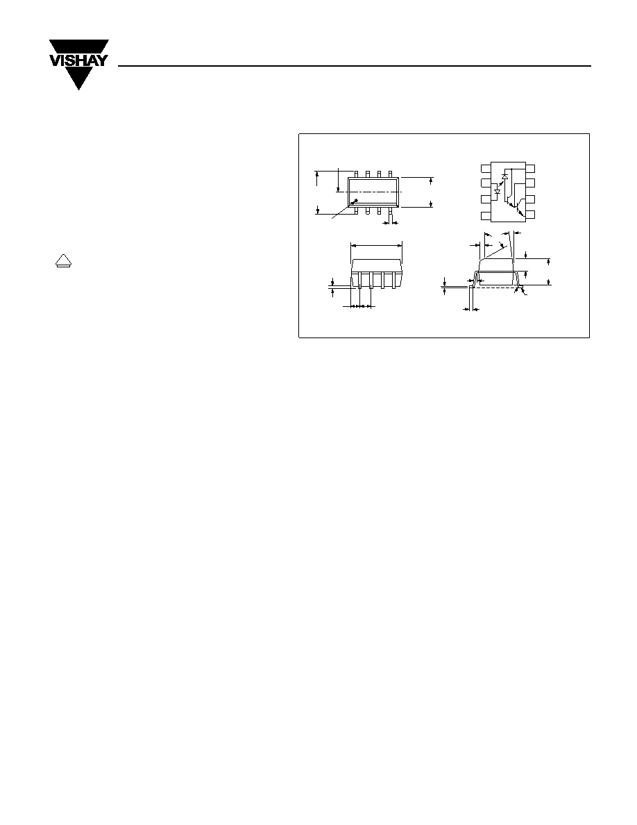
°
Lead
Coplanarity
±.0015 (.04)
max.
.015
±.002
(.38
±.05)
.008 (.20)
7
°
.058
±.005
(1.49
±.13)
.125
±.005
(3.18
± .13)
.050
(1.27)
typ.
.192
±.005
(4.88
±.13)
.004 (.10)
.008 (.20)
.021
(.53)
5
°max.
R.010
(.25)
max.
.020
±.004
(.51
±.10)
2 plcs.
.240
(6.10)
.016
(.41)
Pin 1
.120
± .002
(3.05
± .05)
CL
1
2
3
4
8
7
6
5
.154
±.002
(.391
±.05)
VCC
NC
Anode
Cathode
NC
V0
VB
GND
Tolerance:
±.005 (unless otherwise noted)
Package Dimensions in Inches (mm)
FEATURES
Industry Standard SOIC-8 Surface Mountable
Package
High Current Transfer Ratio, 800%
Low Input Current, 0.5 mA
High Output Current, 60 mA
Isolation Test Voltage, 3000 VRMS
TTL Compatible Output, VOL=0.1 V
Adjustable Bandwidth—Access to Base
Underwriters Lab File #E52744
VDE 0884 Available with Option 1
APPLICATIONS
Logic Ground Isolation—TTL/TTL, TTL/CMOS,
CMOS/CMOS, CMOS/TTL
EIA RS 232C Line Receiver
Low Input Current Line Receiver—Long Lines,
Party Lines
Telephone Ring Detector
117 VAC Line Voltage Status Indication—Low
Input Power Dissipation
Low Power Systems—Ground Isolation
DESCRIPTION
Very high current ratio together with 3000 VRMS isolation
are achieved by coupling an LED with an integrated
high gain photodetector in a SOIC-8 package. Separate
pins for the photodiode and output stage enable TTL
compatible saturation voltages with high speed opera-
tion. Photodarlington operation is achieved by tying the
VCC and VO terminals together. Access to the base ter-
minal allows adjustment to the gain bandwidth.
The SFH6318T is ideal for TTL applications since the
300% minimum current transfer ratio with an LED cur-
rent of 1.6 mA enables operation with one unit load-in
and one unit load-out with a 2.2 k
pull-up resistor.
The SFH6319T is best suited for low power logic appli-
cations involving CMOS and low power TTL. A 400%
current transfer ratio with only 0.5 mA of LED current is
guaranteed from 0
°C to 70°C.
Caution:
Due to the small geometries of this device, it should be han-
dled with Electrostatic Discharge (ESD) precautions. Proper
grounding would prevent damage further and/or degrada-
tion which may be induced by ESD.
V
DE
SFH6318T/6319T
Low Current, High Gain
Optocoupler
相關(guān)PDF資料 |
PDF描述 |
|---|---|
| SFH6326 | 2 CHANNEL LOGIC OUTPUT OPTOCOUPLER, 1 Mbps |
| SFH6326 | 2 CHANNEL LOGIC OUTPUT OPTOCOUPLER, 1 Mbps |
| SFH6326 | 1 CHANNEL LOGIC OUTPUT OPTOCOUPLER, 1 Mbps |
| SFH6345-X001 | 1 CHANNEL LOGIC OUTPUT OPTOCOUPLER, 1 Mbps |
| SFH6345-X017 | 1 CHANNEL LOGIC OUTPUT OPTOCOUPLER, 1 Mbps |
相關(guān)代理商/技術(shù)參數(shù) |
參數(shù)描述 |
|---|---|
| SFH6318T | 制造商:Vishay Semiconductors 功能描述:Optocoupler |
| SFH6319 | 制造商:INFINEON 制造商全稱:Infineon Technologies AG 功能描述:LOW CURRENT, HIGH GAIN OPTOCOUPLER |
| SFH6319 | 制造商:Vishay Intertechnologies 功能描述:OPTOCOUPLER SMD TRANSISTOR O/P |
| SFH6319T | 功能描述:高速光耦合器 100kbd Low Input Current High Gain RoHS:否 制造商:Avago Technologies 電流傳遞比: 最大波特率: 最大正向二極管電壓:1.75 V 最大反向二極管電壓:5 V 最大功率耗散:40 mW 最大工作溫度:+125 C 最小工作溫度:- 40 C 封裝 / 箱體:SOIC-5 封裝:Tube |
| SFH6319-T | 制造商:Vishay Angstrohm 功能描述:Optocoupler DC-IN 1-CH Darlington With Base DC-OUT 8-Pin SOIC N T/R 制造商:Vishay 功能描述:Optocoupler DC-IN 1-CH Darlington With Base DC-OUT 8-Pin SOIC N T/R |
發(fā)布緊急采購,3分鐘左右您將得到回復(fù)。