- 您現(xiàn)在的位置:買賣IC網(wǎng) > PDF目錄66214 > SFH600-3-X001 (VISHAY INTERTECHNOLOGY INC) 1 CHANNEL TRANSISTOR OUTPUT OPTOCOUPLER PDF資料下載
參數(shù)資料
| 型號(hào): | SFH600-3-X001 |
| 廠商: | VISHAY INTERTECHNOLOGY INC |
| 元件分類: | 光電耦合器 |
| 英文描述: | 1 CHANNEL TRANSISTOR OUTPUT OPTOCOUPLER |
| 文件頁(yè)數(shù): | 1/4頁(yè) |
| 文件大?。?/td> | 524K |
| 代理商: | SFH600-3-X001 |
Document Number: 83662
www.vishay.com
Revision 17-August-01
2–217
SFH600
TRIOS Phototransistor Optocoupler
FEATURES
High Current Transfer Ratios
SFH600-0, 40 to 80%
SFH600-1, 63 to 125%
SFH600-2, 100 to 200%
SFH600-3, 160 to 320%
Isolation Test Voltage (1.0 s), 5300 VRMS
VCEsat 0.25 (≤0.4) V, IF=10 mA, IC=2.5 mA
High Quality Premium Device
Long Term Stability
Storage Temperature, –55
° to +150°C
Field Effect Stable by TRIOS (TRansparent
IOn Shield)
Underwriters Lab File #E52744
VDE 0884 Available with Option 1
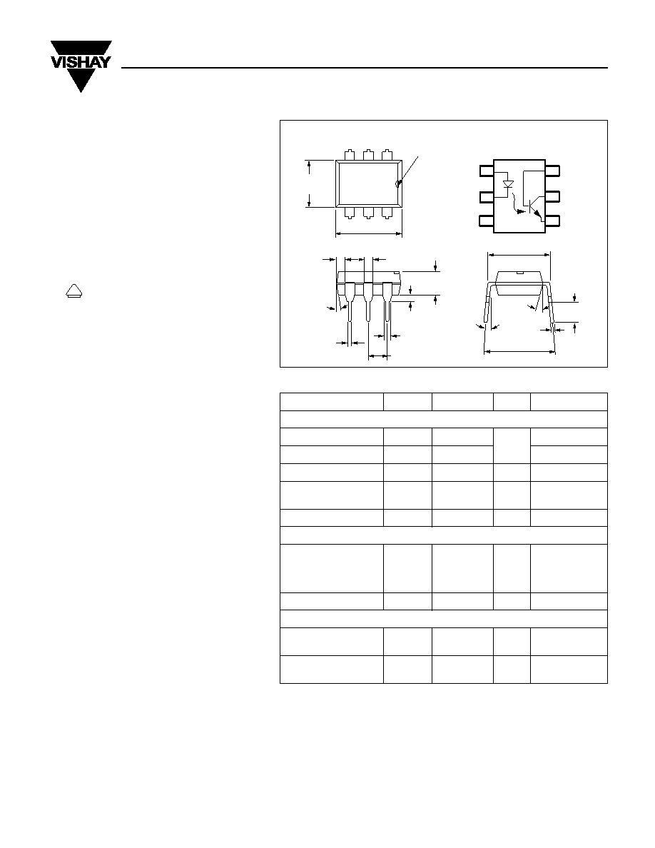
DESCRIPTION
The SFH600 is an optocoupler with a GaAs LED emit-
ter which is optically coupled with a silicon planar pho-
totransistor detector. The component is packaged in a
plastic plug-in case, 20 AB DIN 41866.
The coupler transmits signals between two electri-
cally isolated circuits. The potential difference
between the circuits to be coupled is not allowed to
exceed the maximum permissible insulating voltage.
Maximum Ratings
Emitter
Reverse Voltage ............................................6.0 V
DC Forward Current ....................................60 mA
Surge Forward Current (tp=10 s) ................2.5 A
Total Power Dissipation ............................100 mW
Detector
Collector-Emitter Voltage............................... 70 V
Emitter-Base Voltage.................................... 7.0 V
Collector Currentt........................................50 mA
Collector Current (t=1 ms) ........................100 mA
Power Dissipation ....................................150 mW
Package
Isolation Test Voltage (between emitter and
detector referred to climate DIN 40046,
part 2, Nov. 74) (t=1.0 s) ..................5300 VRMS
Creepage ................................................
≥7.0 mm
Clearance
..................................................... ≥7.0 mm
Isolation Thickness between Emitter &
Detector ..................................................
≥0.4 mm
Comparative Tracking Index per
DIN IEC 112/VDE0303, part 1 ..................... 175
Isolation Resistance
VIO=500 V, TA=25°C ................................ ≥10
12
VIO=500 V, TA=100°C.............................. ≥10
11
Storage Temperature Range......–55
°C to +150°C
Ambient Temperature Range .....–55
°C to +100°C
Junction Temperature ................................. 100
°C
Soldering Temperature (max. 10 s, dip
soldering: distance to seating plane
≥1.5 mm) .................................................260°C
V
DE
Characteristics (TA=25°C)
Symbol
Unit
Condition
Emitter
Forward Voltage
VF
1.25 (
≤1.65)
V
IF=60 mA
Breakdown Voltage
VBR
≥6.0
IR=10 A
Reverse Current
IR
0.01 (
≤10)
A
VR=6.0 V
Capacitance
CO
25
pF
VF=0 V
f=1.0 MHz
Thermal Resistance
RTHJamb
750
K/W
—
Detector
Capacitance
Collector-Emitter
Collector-Base
Emitter-Base
CCE
CCB
CEB
5.2
6.5
9.5
pF
f=1.0 MHz
VCE=5.0 V
VCB=5.0 V
VEB=5.0 V
Thermal Resistance
RTHJamb
500
K/W
—
Package
Saturation Voltage,
Collector-Emitter
VCEsat
0.25 (
≤0.4)
V
IF=10 mA,
IC=2.5 mA
Coupling Capacitance
CIO
0.6
pF
VIO=0
f=1.0 MHz
.010 (.25)
typ.
.114 (2.90)
.130 (3.0)
.130 (3.30)
.150 (3.81)
.031 (0.80) min.
.300 (7.62)
typ.
.031 (0.80)
.035 (0.90)
.100 (2.54) typ.
.039
(1.00)
Min.
.018 (0.45)
.022 (0.55)
.048 (0.45)
.022 (0.55)
.248 (6.30)
.256 (6.50)
.335 (8.50)
.343 (8.70)
pin one ID
6
5
4
1
2
3
18
°
3
°–9°
.300–.347
(7.62–8.81)
4
°
typ.
Dimensions in inches (mm)
1
2
3
6
5
4
Base
Collector
Emitter
Anode
Cathode
NC
相關(guān)PDF資料 |
PDF描述 |
|---|---|
| SFH600-1-X001 | 1 CHANNEL TRANSISTOR OUTPUT OPTOCOUPLER |
| SFH611A | 1 CHANNEL TRANSISTOR OUTPUT OPTOCOUPLER |
| SFH612A | 1 CHANNEL DARLINGTON OUTPUT OPTOCOUPLER |
| SFH655A | 1 CHANNEL DARLINGTON OUTPUT OPTOCOUPLER |
| SFH6156-2SM | 1 CHANNEL TRANSISTOR OUTPUT OPTOCOUPLER |
相關(guān)代理商/技術(shù)參數(shù) |
參數(shù)描述 |
|---|---|
| SFH600-3X006 | 功能描述:晶體管輸出光電耦合器 Phototransistor Out Single CTR>160-320% RoHS:否 制造商:Vishay Semiconductors 輸入類型:DC 最大集電極/發(fā)射極電壓:70 V 最大集電極/發(fā)射極飽和電壓:0.4 V 絕緣電壓:5300 Vrms 電流傳遞比:100 % to 200 % 最大正向二極管電壓:1.65 V 最大輸入二極管電流:60 mA 最大集電極電流:100 mA 最大功率耗散:100 mW 最大工作溫度:+ 110 C 最小工作溫度:- 55 C 封裝 / 箱體:DIP-4 封裝:Bulk |
| SFH600-3X007 | 功能描述:晶體管輸出光電耦合器 Phototransistor Out Single CTR>160-320% RoHS:否 制造商:Vishay Semiconductors 輸入類型:DC 最大集電極/發(fā)射極電壓:70 V 最大集電極/發(fā)射極飽和電壓:0.4 V 絕緣電壓:5300 Vrms 電流傳遞比:100 % to 200 % 最大正向二極管電壓:1.65 V 最大輸入二極管電流:60 mA 最大集電極電流:100 mA 最大功率耗散:100 mW 最大工作溫度:+ 110 C 最小工作溫度:- 55 C 封裝 / 箱體:DIP-4 封裝:Bulk |
| SFH600-4 | 制造商:未知廠家 制造商全稱:未知廠家 功能描述:OPTICALLY COUPLED ISOLATOR PHOTOTRANSISTOR OUTPUT |
| SFH601 | 制造商:VISHAY 制造商全稱:Vishay Siliconix 功能描述:Optocoupler, Phototransistor Output, With Base Connection |
| SFH601_08 | 制造商:VISHAY 制造商全稱:Vishay Siliconix 功能描述:Optocoupler, Phototransistor Output, with Base Connection |
發(fā)布緊急采購(gòu),3分鐘左右您將得到回復(fù)。