- 您現(xiàn)在的位置:買(mǎi)賣(mài)IC網(wǎng) > PDF目錄385838 > SE567FE (NXP SEMICONDUCTORS) Tone decoder/phase-locked loop PDF資料下載
參數(shù)資料
| 型號(hào): | SE567FE |
| 廠(chǎng)商: | NXP SEMICONDUCTORS |
| 元件分類(lèi): | XO, clock |
| 英文描述: | Tone decoder/phase-locked loop |
| 中文描述: | PHASE LOCKED LOOP, CDIP8 |
| 封裝: | CERDIP-8 |
| 文件頁(yè)數(shù): | 7/13頁(yè) |
| 文件大小: | 165K |
| 代理商: | SE567FE |
第1頁(yè)第2頁(yè)第3頁(yè)第4頁(yè)第5頁(yè)第6頁(yè)當(dāng)前第7頁(yè)第8頁(yè)第9頁(yè)第10頁(yè)第11頁(yè)第12頁(yè)第13頁(yè)
Philips Semiconductors Linear Products
Product specification
NE/SE567
Tone decoder/phase-locked loop
April 15, 1992
409
TYPICAL RESPONSE
Response to 100mV
RMS
Tone Burst
Response to Same Input Tone Burst
With Wideband Noise
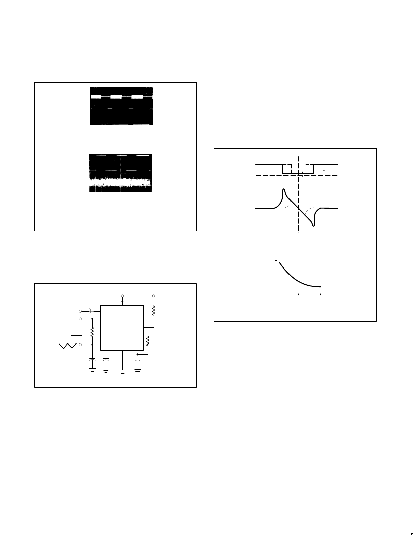
3. The value of C3 is generally non-critical. C3 sets the band edge
of a low-pass filter which attenuates frequencies outside the
detection band to eliminate spurious outputs. If C3 is too small,
frequencies just outside the detection band will switch the output
stage on and off at the beat frequency, or the output may pulse
on and off during the turn-on transient. If C3 is too large, turn-on
and turn-off of the
INPUT
OUTPUT
OUTPUT
INPUT
NOTES:
S/N = –6dB
R
= 100
NOTE:
R
L
= 100
Noise Bandwidth = 140Hz
Figure 1.
INPUT
3
5
6
2
7
1
8
4
+V
+V
OUTPUT
LOW
FILTER
567
R
1
R
L
R
2
C
3
C
2
C
1
fO
1
R1C1
output stage will be delayed until the voltage on C
3
passes the
threshold voltage. (Such delay may be desirable to avoid spurious
outputs due to transient frequencies.) A typical minimum value for
C
3
is 2C
2
.
4. Optional resistor R2 sets the threshold for the largest “no output”
input voltage. A value of 130k
is used to assure the tested limit
of 10mV
RMS
min. This resistor can be referenced to ground for
increased sensitivity. The explanation can be found in the
“optional controls” section which follows.
AVAILABLE OUTPUTS
(Figure 1)
The primary output is the uncommitted output transistor collector,
Pin 8. When an in-band input signal is present, this transistor
saturates; its collector voltage being less than 1.0 volt (typically
0.6V) at full output current (100mA). The voltage at Pin 2 is the
phase detector output which is a linear function of frequency over
the range of 0.95 to 1.05 f
O
with a slope of about 20mV per percent
of frequency deviation. The average voltage at Pin 1 is, during lock,
a function of the in-band input amplitude in accordance with the
transfer characteristic given. Pin 5 is the controlled oscillator square
wave output of magnitude (+V -2V
BE
)
(+V-1.4V) having a DC
average of +V/2. A 1k
load may be driven from pin 5. Pin 6 is an
exponential triangle of 1V
P-P
with an average DC level of +V/2. Only
high impedance loads may be
Figure 2. Typical Output Response
THRESHOLD VOLTAGE
V
REF
4.0
3.5
3.0
2.5
0
100
200mVrms
PIN 1
(AVG)
f
1
= f
O
7%
BW
V
CE
(SAT) < 1.0V
14%
V+
0
3.9V
3.8V
3.7V
1.1f
O
f
O
0.9f
O
LOW PASS
(PIN 2)
OUTPUT
相關(guān)PDF資料 |
PDF描述 |
|---|---|
| SE567 | Tone decoder/phase-locked loop |
| SE567D | Tone decoder/phase-locked loop |
| SE567N | Tone decoder/phase-locked loop |
| SE701 | SILICON GATE ENHANCEMENT MODE RF POWER VDMOS TRANSISTOR |
| SEA Series | SRAM Memory Card 128 kB Through512 kB(128 kB - 512 kB靜態(tài)RAM存儲(chǔ)器卡) |
相關(guān)代理商/技術(shù)參數(shù) |
參數(shù)描述 |
|---|---|
| SE567N | 制造商:PHILIPS 制造商全稱(chēng):NXP Semiconductors 功能描述:Tone decoder/phase-locked loop |
| SE57 | 制造商:MISCELLANEOUS 功能描述: |
| SE-57 | 制造商:USM-EYELETS 功能描述: |
| SE-57 TN | 制造商:USM-EYELETS 功能描述: |
| SE592 | 制造商:TI 制造商全稱(chēng):Texas Instruments 功能描述:differential video amplififiers |
發(fā)布緊急采購(gòu),3分鐘左右您將得到回復(fù)。