- 您現在的位置:買賣IC網 > PDF目錄192727 > SD-14620DX-404L (DATA DEVICE CORP) SYNCHRO OR RESOLVER TO DIGITAL CONVERTER, CQIP54 PDF資料下載
參數資料
| 型號: | SD-14620DX-404L |
| 廠商: | DATA DEVICE CORP |
| 元件分類: | 位置變換器 |
| 英文描述: | SYNCHRO OR RESOLVER TO DIGITAL CONVERTER, CQIP54 |
| 封裝: | 1.500 X 0.780 INCH, 0.210 INCH HEIGHT, HERMETIC SEALED, CERAMIC, DIP-54 |
| 文件頁數: | 6/12頁 |
| 文件大小: | 150K |
| 代理商: | SD-14620DX-404L |
3
Data Device Corporation
www.ddc-web.com
SD-14620
J-04/03-0
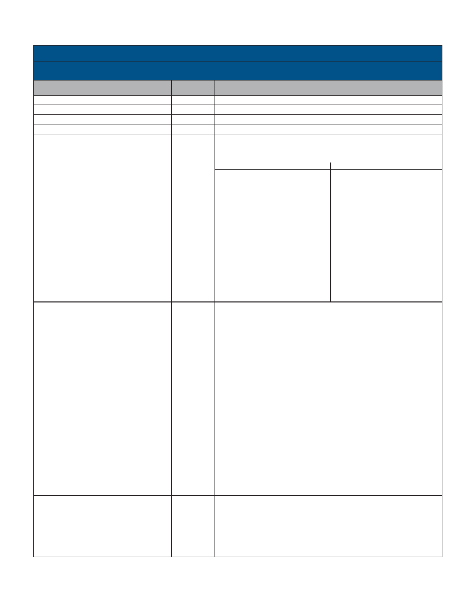
TABLE 1. SD-14620 SERIES SPECIFICATIONS (EACH CHANNEL)
These specs apply over the rated power supply, temperature, and reference frequency ranges;
10% signal amplitude variation, and 10% harmonic distortion.
PARAMETER
UNIT
VALUE
RESOLUTION
Bits
programmable 10, 12, 14, or 16
ACCURACY
Min
±1, ±2 or ±4, + 1 LSB (see TABLE 5)
REPEATABILITY
LSB
1 max.
DIFFERENTIAL LINEARITY
LSB
1 max.
REFERENCE INPUT
Type
SD-14620
Voltage Range
Frequency
Input Impedance
single ended
differential
Common-Mode Range
SD-14620XS
Voltage Range
Frequency
Input Impedance
single ended
differential
Common-Mode Range
±Sig/Ref Phase Shift
Vrms
Hz
Ohm
Vpeak
Vrms
Hz
Ohm
Vpeak
deg.
(RH, RL)
Each Channel
differential
2 & 11.8 V UNITS
90 V UNIT
2-35
10-130
360 - 5K
60 (47-5K)
400 (360-5K)
60K
270K min.
120K
540K min.
50, 100 transient
200, 300 transient
2-35
—
1K - 5K
—
40K
—
80K
—
50, 100 transient
—
45 max
—
SIGNAL INPUT
CHARACTERISTICS
90 V Synchro Input (L-L)
Zin line-to-line
Zin line-to-ground
Common-Mode Voltage
11.8 V Synchro Input (L-L)
Zin line-to-line
Zin line-to-ground
Common-Mode Voltage
11.8 V Resolver Input (L-L)
Zin line-to-line
Zin line-to-ground
Common-Mode Voltage
2 V Direct Input (L-L)
Voltage Range
Max. Voltage w/o Damage
Input Impedance
2 V Resolver Input (L-L)
Zin single ended
Zin differential
Common-Mode Voltage
Ohm
V
Ohm
V
Ohm
V
Vrms
V
Ohm
V
123K
80K
180 max.
52K
34K
30 max.
(same for “S” option)
140K
70K
30 max.
2 nom, 2.3 max.
25 cont, 100 pk transient
20 M || 10 pF min.
(“S” option only)
11K
22K
4.9 max.
DIGITAL INPUT/OUTPUT
Logic Type
INPUTS
TTL/CMOS compatible
Logic 0 = 0.8 V max.
Logic 1 = 2.0 V min.
Loading (per channel) =10 A
max P.U. current source to
+5 V || 5 pF max.
CMOS transient protected.
相關PDF資料 |
PDF描述 |
|---|---|
| SD-14620DX-404S | SYNCHRO OR RESOLVER TO DIGITAL CONVERTER, CQIP54 |
| SD-14620DX-404Y | SYNCHRO OR RESOLVER TO DIGITAL CONVERTER, CQIP54 |
| SD-14620DX-404Z | SYNCHRO OR RESOLVER TO DIGITAL CONVERTER, CQIP54 |
| SD-14620DX-412L | SYNCHRO OR RESOLVER TO DIGITAL CONVERTER, CQIP54 |
| SD-14620DX-412Q | SYNCHRO OR RESOLVER TO DIGITAL CONVERTER, CQIP54 |
相關代理商/技術參數 |
參數描述 |
|---|---|
| SD-14621FS-295 | 制造商:DDC 功能描述: |
| SD1463 | 制造商:STMICROELECTRONICS 制造商全稱:STMicroelectronics 功能描述:RF & MICROWAVE TRANSISTORS VHF/UHF APPLICATIONS |
| SD1468 | 制造商:MICROSEMI 制造商全稱:Microsemi Corporation 功能描述:RF AND MICROWAVE TRANSISTORS WIDEBAND VHF-UHF CLASS C |
| SD14-680 | 制造商:COOPER BUSSMANN 功能描述:Inductor Power Shielded Wirewound 68uH 20% 100KHz Ferrite 474mA 1.11Ohm DCR 2020 T/R 制造商:COOPER BUSSMANN 功能描述:Ind Power Shielded Wirewound 68uH 20% 100KHz Ferrite 474mA 2020 T/R |
| SD14-680-R | 功能描述:固定電感器 68uH 0.449A 1.11ohms RoHS:否 制造商:AVX 電感:10 uH 容差:20 % 最大直流電流:1 A 最大直流電阻:0.075 Ohms 工作溫度范圍:- 40 C to + 85 C 自諧振頻率:38 MHz Q 最小值:40 尺寸:4.45 mm W x 6.6 mm L x 2.92 mm H 屏蔽:Shielded 端接類型:SMD/SMT 封裝 / 箱體:6.6 mm x 4.45 mm |
發(fā)布緊急采購,3分鐘左右您將得到回復。