- 您現(xiàn)在的位置:買賣IC網(wǎng) > PDF目錄271672 > SD-14616-164L (DATA DEVICE CORP) SYNCHRO OR RESOLVER TO DIGITAL CONVERTER, DMA36 PDF資料下載
參數(shù)資料
| 型號(hào): | SD-14616-164L |
| 廠商: | DATA DEVICE CORP |
| 元件分類: | 位置變換器 |
| 英文描述: | SYNCHRO OR RESOLVER TO DIGITAL CONVERTER, DMA36 |
| 封裝: | DDIP-36 |
| 文件頁(yè)數(shù): | 3/6頁(yè) |
| 文件大?。?/td> | 56K |
| 代理商: | SD-14616-164L |

THEORY OF OPERATION
The SDC-14610/15 Series of converters are based upon a sin-
gle chip CMOS custom monolithic. They are implemented using
the latest IC technology which merges precision analog circuitry
with digital logic to form a complete high performance tracking
resolver-to-digital converter.
FIGURE 1 is the Functional Block Diagram of SDC-14610/15
Series. The converter operates with ±5 V dc power supplies.
Analog signals are referenced to analog ground, which is at
ground potential. The converter is made up of three main sec-
tions; an input front-end, a converter, and a digital interface. The
converter front-end differs for synchro, resolver and direct inputs.
An electronic Scott-T is used for synchro inputs, a resolver con-
ditioner for resolver inputs and a sine and cosine voltage follow-
er for direct inputs. These amplifiers feed the high accuracy
Control Transformer (CT). Its other input is the 14-bit digital angle
φ. Its output is an analog error angle, or difference angle,
between the two inputs. The CT performs the ratiometric trigono-
metric computation of SIN
θCOSφ - COSθSINφ = SIN(θ - φ) using
amplifiers, switches, logic and capacitors in precision ratios.
The converter accuracy is limited by the precision of the com-
puting elements in the CT. In these converters ratioed capacitors
are used in the CT, instead of the more conventional precision
ratioed resistors. Capacitors used as computing elements with
op-amps need to be sampled to eliminate voltage drifting.
Therefore, the circuits are sampled at a high rate to eliminate this
drifting and at the same time to cancel out the op-amp offsets.
The error processing is performed using the industry standard
technique for type II tracking R/D converters. The dc error is inte-
grated yielding a velocity voltage which in turn drives a voltage
controlled oscillator (VCO). This VCO is an incremental integra-
tor (constant voltage input to position rate output) which togeth-
er with the velocity integrator forms a type II servo feedback loop.
A lead in the frequency response is introduced to stabilize the
loop and another lag at higher frequency is introduced to reduce
the gain and ripple at the carrier frequency and above.
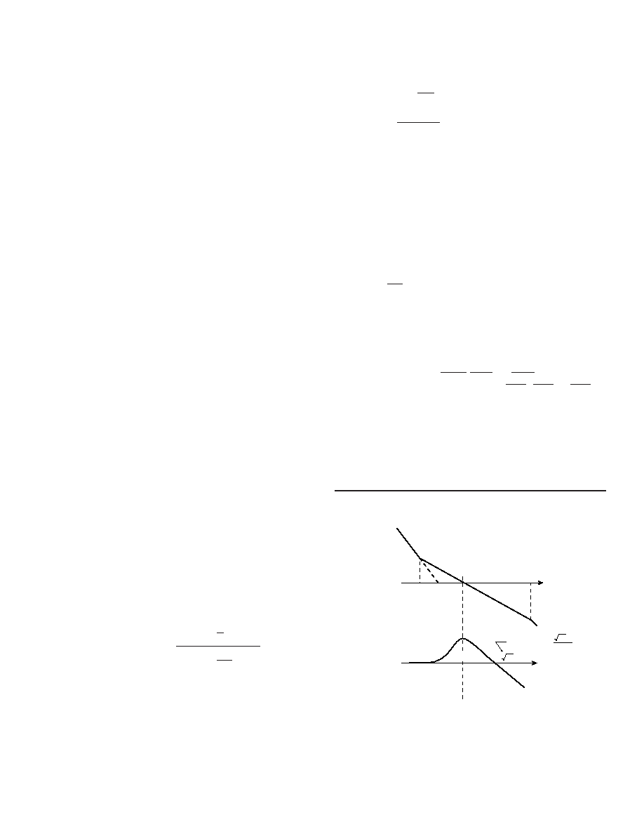
TRANSFER FUNCTION AND BODE PLOT
The dynamic performance of the converter can be determined
from its functional block diagram and its bode plots (open and
closed loop); these are shown in FIGUREs 1 and 2 respectively.
The open loop transfer function is as follows:
S
A2
+1
B
(
)
Open Loop Transfer Function =
S
S2
+1
10B
(
)
where A is the gain coefficient
and B is the frequency of lead compensation
The components of gain coefficient are error gradient, integrator
gain, and VCO gain. These can be broken down as follows:
- Error Gradient = 0.011 volts per LSB (CT+Error Amp+Demod)
1
- Integrator gain =
volts per second per volt
RiCi
1
- VCO Gain =
LSBs per second per volt
1.25 RvCv
GENERAL SETUP CONSIDERATIONS
The following recommendations should be considered when
connecting the SDC-14610/15 Series converters:
1) Power supplies are ±5 V dc. For lowest noise performance it
is recommended that a 0.1 F or larger cap be connected
from each supply to ground near the converter package.
2) Direct inputs are referenced to A GND.
INHIBIT AND ENABLE TIMING
The Inhibit (INH) signal is used to freeze the digital output angle
in the transparent output data latch while data is being trans-
ferred. Application of an Inhibit signal does not interfere with the
continuous tracking of the converter. As shown in FIGURE 3,
angular output data is valid 500 nanoseconds maximum after the
application of the low-going inhibit pulse.
Output angle data is enabled onto the tri-state data bus in six
bytes. The Enable MSB (EM A,EM B, or EM C) is used for the
most significant 8 bits and Enable LSB (EL A, EL B, or EL C) is
used for the least significant bits. As shown in FIGURE 4, output
data is valid 150 nanoseconds maximum after the application of
a low-going enable pulse. The tri-state data bus returns to the
high impedance state 100 nanoseconds maximum after the ris-
ing edge of the enable signal.
3
-12
db/oct
GAIN = 4
B
A
2A
-6 db/oct
10B
ω (rad/sec)
2A
2 2 A
ω (rad/sec)
f
= BW =
3db
2 A (Hz)
π
CLOSED LOOP
OPEN LOOP
- GAIN = 0.4
(B=A/2)
(CRITICALLY DAMPED)
FIGURE 2. BODE PLOTS
相關(guān)PDF資料 |
PDF描述 |
|---|---|
| SDC-14565-382 | SYNCHRO OR RESOLVER TO DIGITAL CONVERTER, DIP36 |
| SDC-14565-392 | SYNCHRO OR RESOLVER TO DIGITAL CONVERTER, DIP36 |
| SD-14619T-192Q | SYNCHRO OR RESOLVER TO DIGITAL CONVERTER, DMA36 |
| SDC-14537-302 | SYNCHRO OR RESOLVER TO DIGITAL CONVERTER, DIP32 |
| SD-14551DX-274 | SYNCHRO OR RESOLVER TO DIGITAL CONVERTER, CQIP34 |
相關(guān)代理商/技術(shù)參數(shù) |
參數(shù)描述 |
|---|---|
| SD1462 | 制造商:MICROSEMI 制造商全稱:Microsemi Corporation 功能描述:RF & MICROWAVE TRANSISTORS WIDEBAND VHF-UHF CLASS C |
| SD-14621FS-295 | 制造商:DDC 功能描述: |
| SD1463 | 制造商:STMICROELECTRONICS 制造商全稱:STMicroelectronics 功能描述:RF & MICROWAVE TRANSISTORS VHF/UHF APPLICATIONS |
| SD1468 | 制造商:MICROSEMI 制造商全稱:Microsemi Corporation 功能描述:RF AND MICROWAVE TRANSISTORS WIDEBAND VHF-UHF CLASS C |
| SD14-680 | 制造商:COOPER BUSSMANN 功能描述:Inductor Power Shielded Wirewound 68uH 20% 100KHz Ferrite 474mA 1.11Ohm DCR 2020 T/R 制造商:COOPER BUSSMANN 功能描述:Ind Power Shielded Wirewound 68uH 20% 100KHz Ferrite 474mA 2020 T/R |
發(fā)布緊急采購(gòu),3分鐘左右您將得到回復(fù)。