- 您現(xiàn)在的位置:買賣IC網(wǎng) > PDF目錄271719 > SD-14615-154S (DATA DEVICE CORP) SYNCHRO OR RESOLVER TO DIGITAL CONVERTER, DMA36 PDF資料下載
參數(shù)資料
| 型號: | SD-14615-154S |
| 廠商: | DATA DEVICE CORP |
| 元件分類: | 位置變換器 |
| 英文描述: | SYNCHRO OR RESOLVER TO DIGITAL CONVERTER, DMA36 |
| 封裝: | DDIP-36 |
| 文件頁數(shù): | 4/6頁 |
| 文件大小: | 56K |
| 代理商: | SD-14615-154S |

4
BIT, BUILT-IN-TEST (OPTIONAL)
This output is a logic line that will flag an internal fault condition,
or LOS (Loss-Of-Signal). The internal fault detector monitors the
internal error and, when it exceeds ±100 LSBs, will set the line
to a logic 0; this condition will occur during a large-step input and
will reset to a logic 1 after the converter settles out. (The error
voltage is filtered with a 500 s filter) BIT will set for an overve-
locity condition because the converter loop can’t maintain
input/output sync. BIT will also be set if a total LOS (loss of all
signals) occurs.
NO FALSE 180° HANGUP
This feature eliminates the “false 180° reading” during instanta-
neous 180° step changes; this condition most often occurs when
the input is “electronically switched” from a digital-to-synchro
converter. If the “MSB” (or 180° bit) is “toggled” on and off, a con-
verter without the “false 180° hangup” feature may fail to
respond.
The condition is artificial, as a “real” synchro or resolver can not
change its output 180° instantaneously. The condition is most
often noticed during wraparound verification tests, simulations,
or troubleshooting.
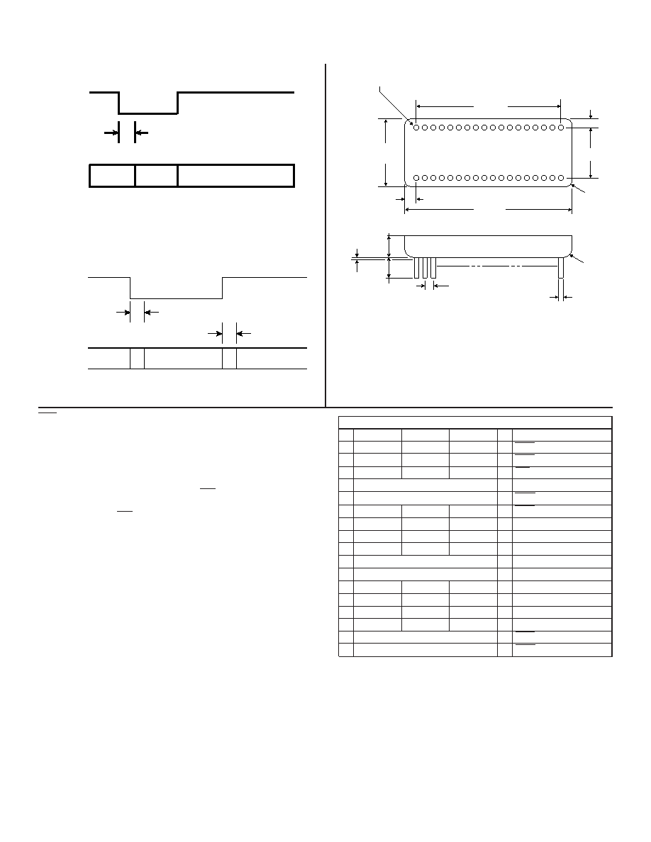
,
ENABLE
150 ns MAX
DATA
VALID
100 ns MAX
HIGH Z
,,,,,,
DATA
VALID
500 ns MAX
INHIBIT
1.895 ±0.005
(48.1 ±0.13)
1.700 ±0.005
(43.2 ±0.13)
0.018 (0.46)
DIAM TYP
0.100 TYP(2.54)
TOL. NON-
CUMULATIVE
0.21 MAX
(5.3)
DOT
IDENTIFIES
PIN 1
0.775 ±0.005
(19.7 ±0.13)
0.600 ±0.005
(15.2 ±0.13)
0.09 ±0.01
(2.3 ±0.25)
0.10 ±0.01
(2.5 ±0.3)
SIDE VIEW
BOTTOM VIEW
0.25 MIN
(6.4)
0.015 MAX
(0.39)
SEATING
PLANE
0.055 (1.4)
RAD TYP
0.086 TYP
RADIUS
TABLE 2. PINOUTS (36 PIN)*
1 S1A(S)
S1A(R)
N.C.
36
2 S2A(S)
S2A(R)
+COSA(D) 36 EM A (Enable MSBs)
3 S3A(S)
S3A(R)
+SINA(D)
34 EL A (Enable LSBs)
4 N.C.
S4A(R)
N.C.
33 INH (Inhibit)
5 GND
(Ground)
32
6 A GND (Analog Ground)
31 EM B (Enable MSBs)
7
S1B(S)
S1B(R)
N.C.
30 EL B (Enable LSBs)
8
S2B(S)
S2B(R)
+COSB(D) 29 Bit 8/Bit 16***
9
S3B(S)
S3B(R)
+SINB(D)
28 Bit 7/Bit 15***
10 N.C.
S4B(R)
N.C.
27 Bit 6/Bit 14
11 -5 V (Power Supply)
26 Bit 5/Bit 13
12 +5 V (Power Supply)
25 Bit 4/Bit 12
13 S1C(S)
S1C(R)
N.C.
24 Bit 3/Bit 11
14 S2C(S)
S2C(R)
+COSC(D) 23 Bit 2/Bit 10
15 S3C(S)
S3C(R)
+SINC(D)
22 Bit 1/Bit 9
16 N.C.
S4C(R)
N.C.
21
17 -REF (-Reference Input)
20 EL C (Enable LSBs)
18 +REF (+Reference Input)
19 EM C (Enable MSBs)
FIGURE 3. INHIBIT TIMING
FIGURE 4. ENABLE TIMING
Notes:
1. Dimensions are in inches (millimeters).
2. Lead identification numbers are for reference only.
3. Lead clusters shall be centered within ±0.01 of outline dimensions. Lead spac-
ing dimensions apply only at seating plane.
4. Pin material meets solderability requirements to MIL-STD-202E, Method 208C.
5. Case is electrically floating.
FIGURE 5. SDC-14610/15 MECHANICAL OUTLINE
Notes: * (S) = Synchro; (R) = Resolver; (D) = 2 V Resolver Direct
** Replaced with BIT - “T” option.
*** Note: SDC-14615 Series only
VEL A (Velocity Output)**
VEL B (Velocity Output)**
VEL C (Velocity Output)**
相關(guān)PDF資料 |
PDF描述 |
|---|---|
| SD-14615-174L | SYNCHRO OR RESOLVER TO DIGITAL CONVERTER, DMA36 |
| SD-14615T-194 | SYNCHRO OR RESOLVER TO DIGITAL CONVERTER, DMA36 |
| SD-14616-164S | SYNCHRO OR RESOLVER TO DIGITAL CONVERTER, DMA36 |
| SD-14616-174 | SYNCHRO OR RESOLVER TO DIGITAL CONVERTER, DMA36 |
| SD-14616-182L | SYNCHRO OR RESOLVER TO DIGITAL CONVERTER, DMA36 |
相關(guān)代理商/技術(shù)參數(shù) |
參數(shù)描述 |
|---|---|
| SD1462 | 制造商:MICROSEMI 制造商全稱:Microsemi Corporation 功能描述:RF & MICROWAVE TRANSISTORS WIDEBAND VHF-UHF CLASS C |
| SD-14621FS-295 | 制造商:DDC 功能描述: |
| SD1463 | 制造商:STMICROELECTRONICS 制造商全稱:STMicroelectronics 功能描述:RF & MICROWAVE TRANSISTORS VHF/UHF APPLICATIONS |
| SD1468 | 制造商:MICROSEMI 制造商全稱:Microsemi Corporation 功能描述:RF AND MICROWAVE TRANSISTORS WIDEBAND VHF-UHF CLASS C |
| SD14-680 | 制造商:COOPER BUSSMANN 功能描述:Inductor Power Shielded Wirewound 68uH 20% 100KHz Ferrite 474mA 1.11Ohm DCR 2020 T/R 制造商:COOPER BUSSMANN 功能描述:Ind Power Shielded Wirewound 68uH 20% 100KHz Ferrite 474mA 2020 T/R |
發(fā)布緊急采購,3分鐘左右您將得到回復(fù)。