- 您現(xiàn)在的位置:買(mǎi)賣(mài)IC網(wǎng) > PDF目錄192631 > SD-14596F3-542L (DATA DEVICE CORP) SYNCHRO OR RESOLVER TO DIGITAL CONVERTER, CDFP36 PDF資料下載
參數(shù)資料
| 型號(hào): | SD-14596F3-542L |
| 廠商: | DATA DEVICE CORP |
| 元件分類(lèi): | 位置變換器 |
| 英文描述: | SYNCHRO OR RESOLVER TO DIGITAL CONVERTER, CDFP36 |
| 封裝: | CERAMIC, FP-36 |
| 文件頁(yè)數(shù): | 11/14頁(yè) |
| 文件大小: | 416K |
| 代理商: | SD-14596F3-542L |
第1頁(yè)第2頁(yè)第3頁(yè)第4頁(yè)第5頁(yè)第6頁(yè)第7頁(yè)第8頁(yè)第9頁(yè)第10頁(yè)當(dāng)前第11頁(yè)第12頁(yè)第13頁(yè)第14頁(yè)
6
updated, CB is at logic 0 and the INH latch is transparent; when
CB goes to logic 1, the INH latch is locked. If CB occurs after INH
has been applied, the latch will remain locked and its data will not
change until CB returns to logic 0; if INH is applied during CB,
the latch will not lock until the CB pulse is over. The purpose of
the 50 ns delay is to prevent a race condition between CB and
INH where the up-down counter begins to change as an INH is
applied.
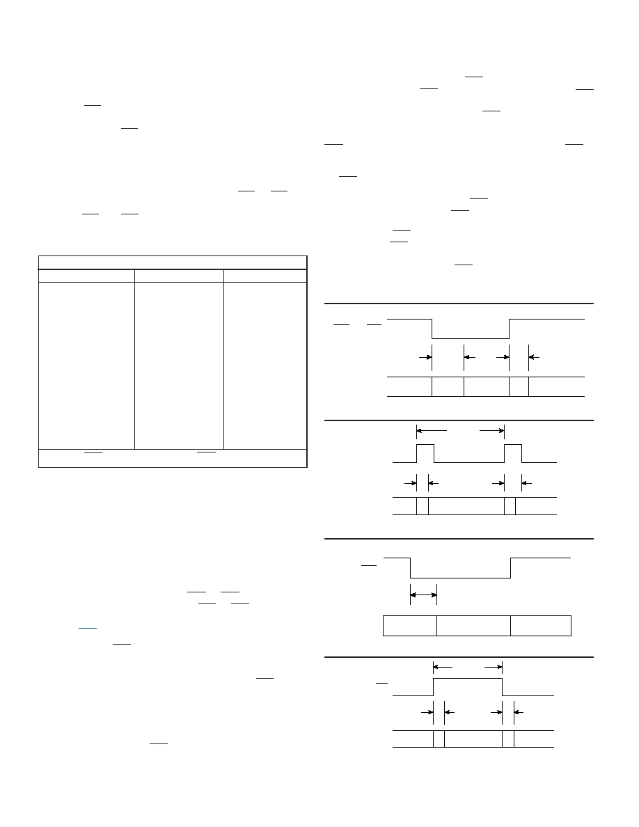
An INH input, regardless of its duration, does not affect the con-
verter update. A simple method of interfacing to a computer
asynchronous to CB is: (1) Apply INH; (2) Wait 0.5
s min; (3)
Transfer the data; (4) Release INH (see FIGURE 9).
A logic 1 for the INH enables the output data to be updated. The
time it takes for INH to go to a logic 1 should be 100 ns minimum
before valid data is transferred. To allow the update of the output
data with valid information the INH must remain at a logic 1 for
1
s minimum (see FIGURE 10 below).
DIGITAL ANGLE OUTPUTS (LOGIC INPUT/OUTPUT)
The digital angle outputs are buffered and provided in a two-byte
format. The first byte contains the MSBs (bits 1-8) and is enabled
by placing HBE (pin 35) to a logic 0. Depending on the user pro-
grammed resolution, the second byte contains the LSBs and is
enabled by placing LBE (pin 17) to a logic 0.
The second byte will contain either bits 9-14 (14-bit resolution) or
bits 9-16 (16-bit resolution). All unused LSBs will be at logic 0.
TABLE 3 lists the angular weight for the digital angle outputs.
The digital angle outputs are valid 150 ns after HBE or LBE are
activated with a logic 0 and are high impedance within 100 ns
max after HBE and LBE are set to logic 1 (see FIGURE 7). Both
enables are internally pulled down.
DIGITAL ANGLE OUTPUT TIMING
The digital angle output is 14 or 16 parallel data bits and
CONVERTER BUSY (CB). All logic outputs are short-circuit
proof to ground and +5 V. The CB output is a positive, 0.8 to
3.0
s pulse.
The digital output data changes approximately 50 ns after the
leading edge of the CB pulse because of an internal delay. Data
is valid 0.2
s after the leading edge of CB (see FIGURE 8). The
angle is determined by the sum of the bits at logic 1. The digital
outputs are valid 150 ns max after HBE or LBE go low and are
high impedance within 100 ns max of HBE or LBE going high.
INHIBIT (INH, PIN 13)
When an Inhibit (INH) input is applied to the SD-14595/96/97,
the Output Transparent Latch is locked causing the output data
bits to remain stable while data is being transferred (see FIG-
URE 9). The output data bits are stable 0.5
s after INH goes to
logic 0.
A logic 0 at the input of the Inhibit Transparent Latch latches the
data, and a logic 1 applied, allows the bits to change. This latch
also prevents the transmission of invalid data when there is an
overlap between CB and INH. While the counter is not being
,
DEPENDS ON d
φ/dt
0.8-3.0
s
CB
0.2
s
DATA
VALID
6.1
s MIN
,,
,
0.5 s
INH
100 ns MIN
DATA
UPDATE
STABLE
1 s MIN
,,
DATA
VALID
0.5
s
ASYNCHROUS TO CB
INH
,,,,
100 ns MAX
HBE OR LBE
150 ns MIN
OUTPUT
VALID
HIGH Z
FIGURE 8. CONVERTER BUSY TIMING DIAGRAM
FIGURE 7. TRI-STATE OUTPUT TIMING
FIGURE 10. OUTPUT DATA UPDATE TIMING
FIGURE 9. INHIBIT TIMING DIAGRAM
TABLE 2. DIGITAL ANGLE OUTPUTS
BIT
DEG/BIT
MIN/BIT
1(MSB)
2
3
4
5
6
7
8
9
10
11
12
13
14(LSB 14 BIT MODE)
15
16(LSB 16 BIT MODE)
180
90
45
22.5
11.25
5.625
2.813
1.405
0.7031
0.3516
0.1758
0.0879
0.0439
0.0220
0.0110
0.0055
10800
5400
2700
1350
675
337.5
168.75
84.38
42.19
21.09
10.55
5.27
2.64
1.32
0.66
0.33
Note: HBE enables the 8 MSBs and LBE enables the LSBs.
相關(guān)PDF資料 |
PDF描述 |
|---|---|
| SD-14596F3-542Q | SYNCHRO OR RESOLVER TO DIGITAL CONVERTER, CDFP36 |
| SD-14596F3-542S | SYNCHRO OR RESOLVER TO DIGITAL CONVERTER, CDFP36 |
| SD-14596F3-542 | SYNCHRO OR RESOLVER TO DIGITAL CONVERTER, CDFP36 |
| SD-14596F3-544K | SYNCHRO OR RESOLVER TO DIGITAL CONVERTER, CDFP36 |
| SD-14596F3-544L | SYNCHRO OR RESOLVER TO DIGITAL CONVERTER, CDFP36 |
相關(guān)代理商/技術(shù)參數(shù) |
參數(shù)描述 |
|---|---|
| SD-14597D1-102 | 制造商:未知廠家 制造商全稱(chēng):未知廠家 功能描述:Synchro-to-Digital Converter |
| SD-14597D1-104 | 制造商:未知廠家 制造商全稱(chēng):未知廠家 功能描述:Synchro-to-Digital Converter |
| SD-14597D1-105 | 制造商:未知廠家 制造商全稱(chēng):未知廠家 功能描述:Synchro-to-Digital Converter |
| SD-14597D1-112 | 制造商:未知廠家 制造商全稱(chēng):未知廠家 功能描述:Synchro-to-Digital Converter |
| SD-14597D1-114 | 制造商:未知廠家 制造商全稱(chēng):未知廠家 功能描述:Synchro-to-Digital Converter |
發(fā)布緊急采購(gòu),3分鐘左右您將得到回復(fù)。