- 您現(xiàn)在的位置:買賣IC網(wǎng) > PDF目錄219717 > SD-14592D4-104 (DATA DEVICE CORP) SYNCHRO OR RESOLVER TO DIGITAL CONVERTER, MDMA36 PDF資料下載
參數(shù)資料
| 型號: | SD-14592D4-104 |
| 廠商: | DATA DEVICE CORP |
| 元件分類: | 位置變換器 |
| 英文描述: | SYNCHRO OR RESOLVER TO DIGITAL CONVERTER, MDMA36 |
| 封裝: | DIP-36 |
| 文件頁數(shù): | 8/12頁 |
| 文件大小: | 120K |
| 代理商: | SD-14592D4-104 |
mable: 1-8 (MSB’s) are enabled by signal EM, 9-14 (LSB’s 14 bit)
or 9-16 (LSB’s 16 bit) are enabled by the signal EL. Outputs are
valid (logic “1” or “0”) 150 ns max after setting EM or EL low, and
are high impedance within 100 ns max of setting EM or EL high.
Both EM and EL are internally pulled-down to +5 V at 30 A max.
The inhibit (INH) input locks the transparent latch so the bits will
remain stable while data is being transferred (See FIGURE 1).
The output is stable 0.5 s after INH is driven to logic “0,” see FIG-
URE 4. A logic “0” at the T input latches the data, and a logic “1”
applied to T will allow the bits to change. The inhibit transparent
latch prevents the transmission of invalid data when there is an
overlap between CB and INH. While the counter is not being
updated, CB is at logic “0” and the INH latch is transparent.
When CB goes to logic “1,” the INH latch is locked. If CB occurs
after INH has been applied, the latch will remain locked and its
data will not change until CB returns to logic “0.” If INH is applied
during CB, the latch will not lock until the CB pulse is over. The
purpose of the 50 ns delay is to prevent a race condition between
CB and INH where the up-down counter begins to change as an
INH is applied. Whenever an input angle change occurs, the
converter changes the digital angle in 1 LSB steps and gener-
ates a converter busy pulse. Output data change is initiated by
the leading edge of the CB pulse, delayed by 50 ns, nominal.
Valid data is available at the outputs 0.2 s after the leading
edge of CB, see FIGURE 5.
RESOLUTION CONTROL
Resolution control is via one logic input A. The SD-14590 (not
the SD-14591 or SD-14592) has programmable resolution.
BUILT-IN-TEST
The Built-ln-Test output (BIT) monitors the level of error (D) from
the demodulator. D represents the difference in the input and
output angles and ideally should be zero. If it exceeds approxi-
mately 65 LSBs (of the selected resolution), the logic level at BIT
will change from a logic 0 to logic 1. This condition will occur dur-
ing a large step and reset after the converter settles out. BIT will
also change to logic 1 for an over-velocity condition, because the
converter loop cannot maintain input-output and/or if the con-
verter malfunctions where it cannot maintain the loop at a null.
BIT will also be set if a total Loss-of-Signal (LOS) and/or a Loss-
of-Reference (LOR) occurs.
DYNAMIC PERFORMANCE
A Type II servo loop (Kv =
∞) and very high acceleration con-
stants give the SD-14590 superior dynamic performance, as list-
ed in TABLE 3. If the power supply voltages are not the ±15 VDC
nominal values, the specified input rates will increase or
decrease in proportion to the fractional change in voltage. A
Control Loop Block Diagram is shown in FIGURE 6, and an
Open Loop Bode Plot is shown in FIGURE 7. The values of the
transfer function coefficients are shown in TABLE 3.
An inhibit input, regardless of its duration, does not affect the
converter update. A simple method of interfacing to a computer
asynchronously to CB is: (A) apply the inhibit, (B) wait 0.5 s
minimum, (C) transfer the data and (D) release the inhibit.
As long as the converter maximum tracking rate is not exceed-
ed, there will be no lag in the converter output. If a step input
5
;
DEPENDS ON d
φ/dt
0.4-2.0
s
CB
0.2
s
DATA
VALID
6.1
s MIN
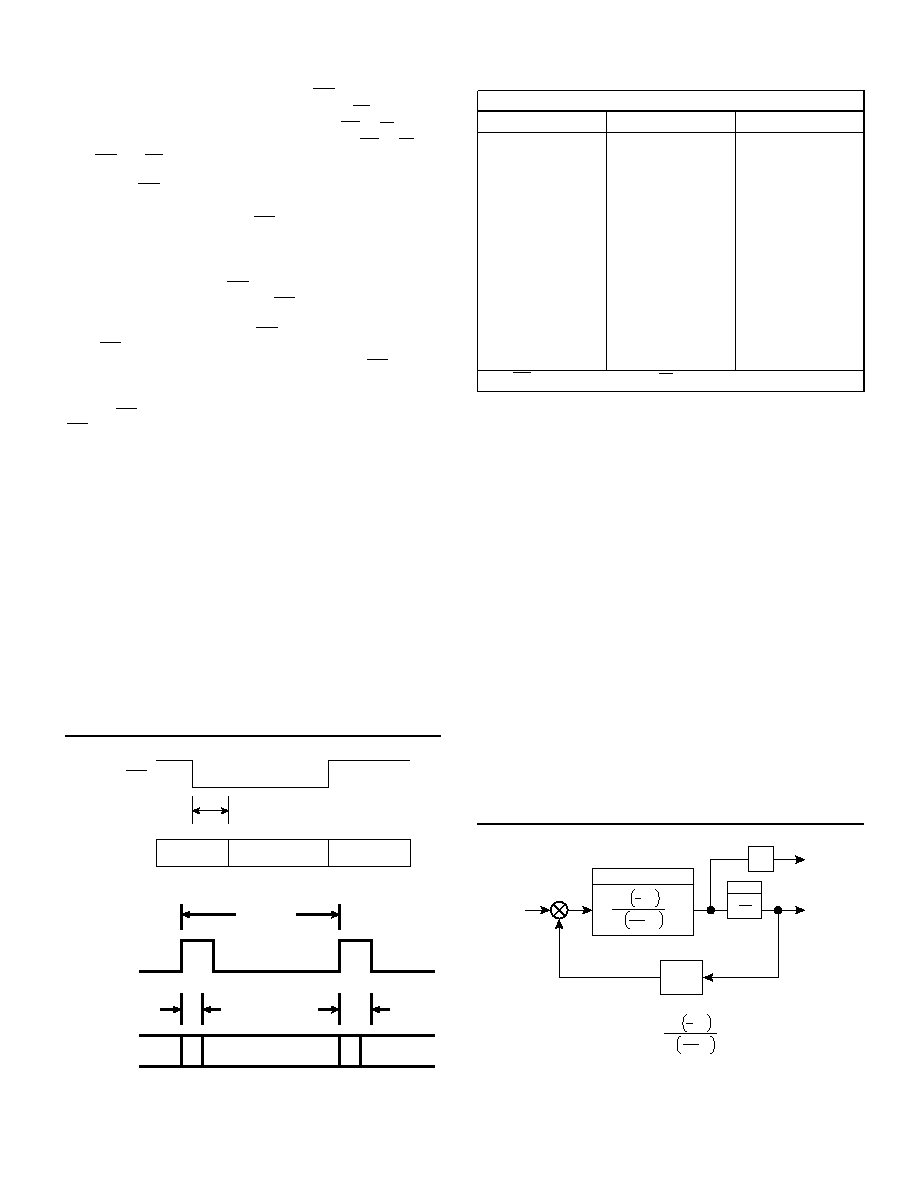
FIGURE 5. CONVERTER BUSY TIMING DIAGRAM
;;
DATA
VALID
0.5
s
ASYNCHRONOUS TO CB
INH
FIGURE 4. INHIBIT TIMING DIAGRAM
TABLE 2. DIGITAL ANGLE OUTPUTS
BIT
DEG/BIT
MIN/BIT
1 MSB
2
3
4
5
6
7
8
9
10
11
12
13
14
15
16
180
90
45
22.5
11.25
5.625
2.813
1.405
0.7031
0.3516
0.1758
0.0879
0.0439
0.0220
0.0110
0.0055
10,800
5,400
2,700
1,350
675
387.5
168.75
84.38
42.19
21.09
10.55
5.27
2.64
1.32
0.66
0.33
Note: EM enables the MSBs and EL enables the LSBs.
ERROR PROCESSOR
INPUT
θ
Open Loop Transfer function = Output
WHERE:
2
A = A A
1
2
VELOCITY
OUT
DIGITAL
POSITION
OUT
(
φ)
VCO
CT
S
A
+ 1
1
B
S
+ 1
10B
H = 1
2
S
A
+ 1
B
2
S
+ 1
10B
+
-
e
A
2
S
2.75
FIGURE 6. CONTROL LOOP BLOCK DIAGRAM
相關(guān)PDF資料 |
PDF描述 |
|---|---|
| SD-14592D4-105 | SYNCHRO OR RESOLVER TO DIGITAL CONVERTER, MDMA36 |
| SD-14592D4-112 | SYNCHRO OR RESOLVER TO DIGITAL CONVERTER, MDMA36 |
| SD-14592D4-114 | SYNCHRO OR RESOLVER TO DIGITAL CONVERTER, MDMA36 |
| SD-14592D4-115 | SYNCHRO OR RESOLVER TO DIGITAL CONVERTER, MDMA36 |
| SD-14592D4-122 | SYNCHRO OR RESOLVER TO DIGITAL CONVERTER, MDMA36 |
相關(guān)代理商/技術(shù)參數(shù) |
參數(shù)描述 |
|---|---|
| SD-14595D1-102 | 制造商:未知廠家 制造商全稱:未知廠家 功能描述:Synchro-to-Digital Converter |
| SD-14595D1-104 | 制造商:未知廠家 制造商全稱:未知廠家 功能描述:Synchro-to-Digital Converter |
| SD-14595D1-105 | 制造商:未知廠家 制造商全稱:未知廠家 功能描述:Synchro-to-Digital Converter |
| SD-14595D1-112 | 制造商:未知廠家 制造商全稱:未知廠家 功能描述:Synchro-to-Digital Converter |
| SD-14595D1-114 | 制造商:未知廠家 制造商全稱:未知廠家 功能描述:Synchro-to-Digital Converter |
發(fā)布緊急采購,3分鐘左右您將得到回復(fù)。