- 您現(xiàn)在的位置:買賣IC網(wǎng) > PDF目錄192488 > SD-14554FX-382L (DATA DEVICE CORP) SYNCHRO OR RESOLVER TO DIGITAL CONVERTER, CDMA34 PDF資料下載
參數(shù)資料
| 型號(hào): | SD-14554FX-382L |
| 廠商: | DATA DEVICE CORP |
| 元件分類: | 位置變換器 |
| 英文描述: | SYNCHRO OR RESOLVER TO DIGITAL CONVERTER, CDMA34 |
| 封裝: | CERAMIC, FP-34 |
| 文件頁(yè)數(shù): | 8/12頁(yè) |
| 文件大?。?/td> | 115K |
| 代理商: | SD-14554FX-382L |
5
Data Device Corporation
www.ddc-web.com
SD-14550 Series
Rev. H
INTERFACING
SOLID-STATE BUFFER PROTECTION - TRANSIENT
VOLTAGE SUPPRESSION
The solid-state signal and reference inputs are true differential
inputs with high AC and DC common rejection, so most applica-
tions will not require units with isolation transformers. Input
impedance is maintained with power off. The recurrent AC peak
+ DC common mode voltage should not exceed the values in
TABLE 1.
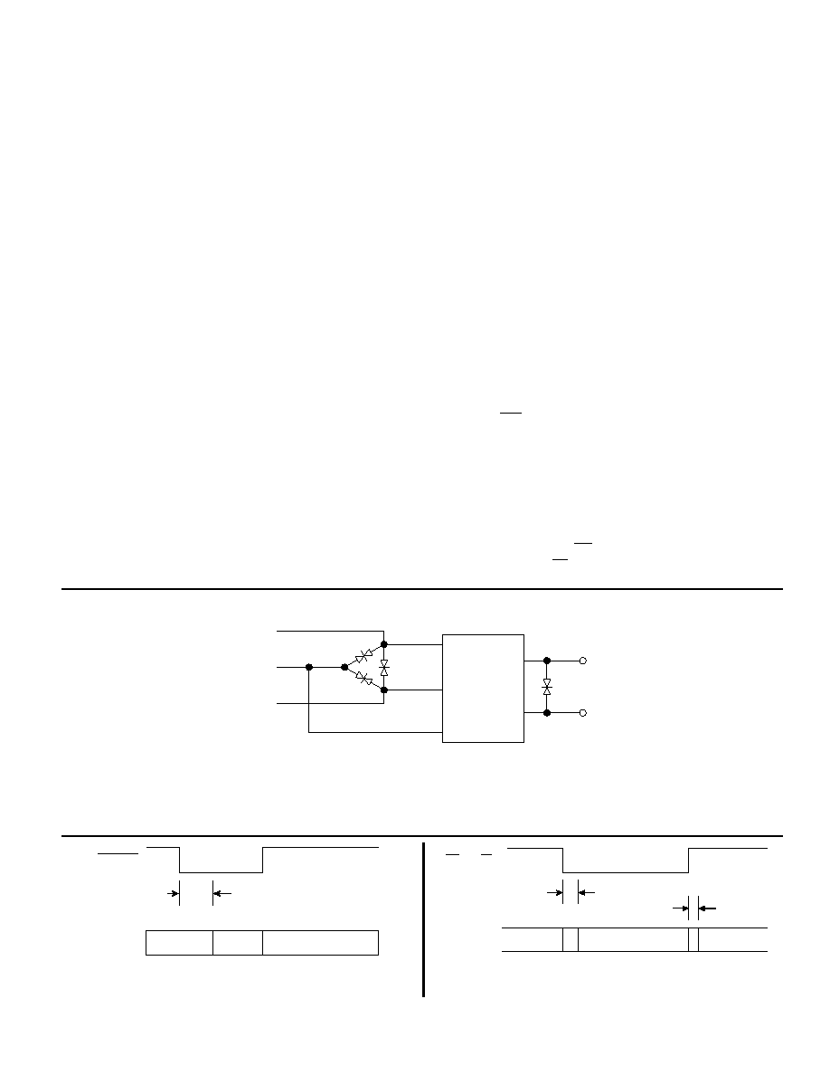
The 90 V line-to-line systems may have voltage transients which
exceed the 300 V specification listed in TABLE 1. These tran-
sients can destroy the thin-film input resistor network in the
hybrid. Therefore, 90 V L-L solid-state input modules may be
protected by installing voltage suppressors as shown in FIGURE
2. Voltage transients are likely to occur whenever a synchro is
switched on and off. For instance, a 1000 V transient can be gen-
erated when the primary of a CX or TX input is opened.
INHIBIT AND ENABLE TIMING
The Inhibit (INH) signal is used to freeze the digital output angle
in the transparent output data latch while the data is being trans-
ferred. Application of an inhibit signal does not interfere with the
continuous tracking of the converter. As shown in FIGURE 3,
angular output data is valid 500 nanoseconds maximum after
the application of the low-going inhibit pulse.
Output angle data is enabled onto the tri-state data bus in 2
bytes. This Enable MSB (EM) is used for the most significant 8
bits and Enable LSB (EL) is used for the least significant bits. As
NO FALSE 180° HANGUP
This feature eliminates the “false 180° reading” during instanta-
neous 180° step changes; this condition most often occurs when
the input is “electronically switched” from a digital-to-synchro
converter. If the “MSB” (or 180° bit) is “toggled” on and off, a
converter without the “false 180° hangup” feature may fail to
respond.
The condition is artificial, as a “real” synchro or resolver cannot
change its output 180° instantaneously. The condition is most
often noticed during wraparound verification tests, simulations,
or troubleshooting.
SYNTHESIZED REFERENCE
The synthesized reference section (“S” option) eliminates errors
due to phase shift between the reference and signal inputs.
Quadrature voltages in a resolver or synchro are by definition
the resulting 90° fundamental signal in the nulled out error volt-
age (e) in the converter. Due to the inductive nature of synchros
and resolvers, their output signals lead the reference input sig-
nal (RH and RL). When an uncompensated reference signal is
used to demodulate the control transformer’s output, quadrature
voltages are not completely eliminated. As shown in FIGURE 1,
the converter synthesizes its own internal reference signal
based on the SIN and COS signal inputs. Therefore, the phase
of the synthesized (internal) reference is determined by the sig-
nal input, resulting in reduced quadrature errors. The synthe-
sized reference circuit also eliminates the 180 degree false error
null hang up.
;;
;
100 ns MAX
EM OR EL
150 ns MAX
DATA
VALID
HIGH Z
;;
;;;
DATA
VALID
500 ns max
INHIBIT
RH
RL
115 V
REF.
INPUT
CR1
CR3
CR2
1N6071A
FOR 90 V SYNCHRO INPUTS
90 V
SYNCHRO
INPUT
S1
HYBRID
S3
S2
CR1, CR2, AND CR3 ARE IN6068A, BIPOLAR TRANSIENT
VOLTAGE SUPRESSORS OR EQUIVALENT.
S1
S3
S2
FIGURE 2. CONNECTIONS FOR VOLTAGE TRANSIENT SUPPRESSORS
FIGURE 4. ENABLE TIMING
FIGURE 3. INHIBIT TIMING
相關(guān)PDF資料 |
PDF描述 |
|---|---|
| SD-14554FX-382Q | SYNCHRO OR RESOLVER TO DIGITAL CONVERTER, CDMA34 |
| SD-14554FX-382W | SYNCHRO OR RESOLVER TO DIGITAL CONVERTER, CDMA34 |
| SD-14554FX-382Y | SYNCHRO OR RESOLVER TO DIGITAL CONVERTER, CDMA34 |
| SD-14554FX-382 | SYNCHRO OR RESOLVER TO DIGITAL CONVERTER, CDMA34 |
| SD-14554FX-384K | SYNCHRO OR RESOLVER TO DIGITAL CONVERTER, CDMA34 |
相關(guān)代理商/技術(shù)參數(shù) |
參數(shù)描述 |
|---|---|
| SD1456 | 功能描述:射頻雙極電源晶體管 NPN 28V 170-230MHz RoHS:否 制造商:M/A-COM Technology Solutions 配置:Single 直流集電極/Base Gain hfe Min:40 最大工作頻率:30 MHz 集電極—發(fā)射極最大電壓 VCEO:25 V 發(fā)射極 - 基極電壓 VEBO:4 V 集電極連續(xù)電流:20 A 最大直流電集電極電流: 功率耗散:250 W 封裝 / 箱體:Case 211-11 封裝:Tray |
| SD1457 | 功能描述:射頻放大器 RF Bipolar Trans RoHS:否 制造商:Skyworks Solutions, Inc. 類型:Low Noise Amplifier 工作頻率:2.3 GHz to 2.8 GHz P1dB:18.5 dBm 輸出截獲點(diǎn):37.5 dBm 功率增益類型:32 dB 噪聲系數(shù):0.85 dB 工作電源電壓:5 V 電源電流:125 mA 測(cè)試頻率:2.6 GHz 最大工作溫度:+ 85 C 安裝風(fēng)格:SMD/SMT 封裝 / 箱體:QFN-16 封裝:Reel |
| SD1458 | 功能描述:射頻放大器 RF Bipolar Trans RoHS:否 制造商:Skyworks Solutions, Inc. 類型:Low Noise Amplifier 工作頻率:2.3 GHz to 2.8 GHz P1dB:18.5 dBm 輸出截獲點(diǎn):37.5 dBm 功率增益類型:32 dB 噪聲系數(shù):0.85 dB 工作電源電壓:5 V 電源電流:125 mA 測(cè)試頻率:2.6 GHz 最大工作溫度:+ 85 C 安裝風(fēng)格:SMD/SMT 封裝 / 箱體:QFN-16 封裝:Reel |
| SD1459 | 功能描述:射頻雙極電源晶體管 NPN 28V 170-230MHz RoHS:否 制造商:M/A-COM Technology Solutions 配置:Single 直流集電極/Base Gain hfe Min:40 最大工作頻率:30 MHz 集電極—發(fā)射極最大電壓 VCEO:25 V 發(fā)射極 - 基極電壓 VEBO:4 V 集電極連續(xù)電流:20 A 最大直流電集電極電流: 功率耗散:250 W 封裝 / 箱體:Case 211-11 封裝:Tray |
| SD-14595D1-102 | 制造商:未知廠家 制造商全稱:未知廠家 功能描述:Synchro-to-Digital Converter |
發(fā)布緊急采購(gòu),3分鐘左右您將得到回復(fù)。