- 您現(xiàn)在的位置:買賣IC網(wǎng) > PDF目錄231053 > SD-14531F5-404S (DATA DEVICE CORP) SYNCHRO OR RESOLVER TO DIGITAL CONVERTER, CDMA36 PDF資料下載
參數(shù)資料
| 型號: | SD-14531F5-404S |
| 廠商: | DATA DEVICE CORP |
| 元件分類: | 位置變換器 |
| 英文描述: | SYNCHRO OR RESOLVER TO DIGITAL CONVERTER, CDMA36 |
| 封裝: | CERAMIC, FP-36 |
| 文件頁數(shù): | 10/16頁 |
| 文件大小: | 170K |
| 代理商: | SD-14531F5-404S |
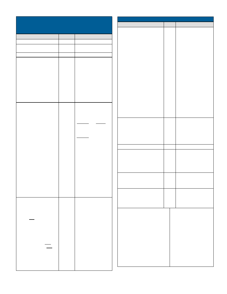
3
Data Device Corporation
www.ddc-web.com
SD-14531
TTL/CMOS compatible
Logic 0 = 0.8 V max.
Logic 1 = 2.0 V min.
Loading = 30 A max.
Logic 0 inhibits Data stable
within 0.5 s (pull up)
Logic 1 for 14 bits
Logic 0 for 16 Bits
(Pull-up current source to
+5 V || 5 pF max CMOS
transient protected)
Logic 0 enables
Data Valid within 150 ns
Logic 1 = High Z
Data High Z within 100 ns
Pull-down current source
to GND || 5 pF max CMOS
transient protected
DIGITAL INPUT/OUTPUT
Logic Type
INPUTS:
Inhibit (INH)
Resolution Control (14B)
(for Programmable Units
Only)
Enable Bits 1 to 8 (HBE)
Enable Bits 9 to 16 (LBE)
(9 to 14 for 14-bit mode)
0.2 max
11.8 VL-L
90 VL-L
60k
500k
30k
250k
30 max
180 max
11.8 VL-L
30k
60k
30k
30 max
Sin and Cos resolver signals
referenced to converter inter-
nal DC reference V.
1 V nominal, 1.15 V max.
15 V continuous
100 V Peak Transient
Zin > 20M || 10pf voltage
follower
60 typ, 45 guaranteed
%
V
Ohm
V
Ohm
V
Vrms
Ohm
Deg
SIGNAL INPUT
CHARACTERISTICS
(voltage options and minimum
input impedance )
Input Impedance Imbalance
! Synchro mode
Zin Line-to-Line
Zin Each Line-to-Gnd
Common Mode Range
! Resolver mode
Zin Single Ended
Zin Differential
Zin Each Line-to Gnd
Common Mode Range
! Direct (1.0 VL-L)
Input Signal Type
Sin/Cos Voltage Range
Max Voltage w/o Damage
Input Impedance
REFERENCE SYNTHESIZER
± Sig/Ref Phase Shift
47-1000 (60 Hz Unit)
360-1000 (400 Hz Unit)
4-130 (for 11.8 V or 90 V
signal input)
3-100 (for 1 V direct signal
input)
250k min
500k min
250 peak max
Hz
Vrms
Ohm
V
REFERENCE INPUT
CHARACTERISTICS
Carrier Frequency Range
Voltage Range
Input Impedance:
! Single Ended
! Differential
Common Mode Range
1 max
LSB
REPEATABILITY
5.2, 2.6, 1.6, or 1.3 (See
note 3)
Min
ACCURACY
14 or 16 (See note 1)
Bits
RESOLUTION
VALUE
UNIT
PARAMETER
TABLE 1. SD-14531 SPECIFICATIONS
Specifications apply over temperature range, power supply range, reference fre-
quency, and amplitude range; 15% signal amplitude variation, up to 10% har-
monic distortion in the reference, and up to 45° of signal to reference phase shift.
TRANSFORMER
CHARACTERISTICS
(See ordering information for list of
Transformers.
Reference Transformers are Optional
for Both Solid-State and Voltage
Follower Input Options.)
400 Hz TRANSFORMERS
Reference Transformer
Carrier Frequency Range
Voltage Range
Input Impedance
Breakdown Voltage to GND
SIGNAL TRANSFORMER
Carrier Frequency Range
Breakdown Voltage to GND
36-Pin DDIP
1.9 x 0.78 x 0.21
(48 x 20 x 5.3)
0.7 max (20)
in
(mm)
oz(g)
PHYSICAL CHARACTERISTICS
Type
Size
Weight
-55 to +125
0 to 70
-65 to +150
°C
TEMPERATURE RANGES
Operating (-1XXX or -4XXX)
(-3XXX or -8XXX)
Storage
+5
±10
+7
25 max+digital output load
V
%
V
mA
POWER SUPPLY
CHARACTERISTICS
Nominal Voltage
Voltage Tolerance
Max Voltage w/o Damage
Current
360 - 1000 Hz
18 - 130 V
40 k
min
1200 V peak
360-1000 Hz
700 V peak
See TABLE 6.
+4.3 V nom
See TABLE 4.
3.5 per LSB of error
1.75 per LSB of error
1
mVrms
mA
DYNAMIC CHARACTERISTICS
ANALOG OUTPUT
Analog Return (V)
Velocity (VEL) (See note 2)
AC error (e)
! 14-Bit Mode
! 16-Bit Mode
Load
Bits
s
DIGITAL INPUT/OUTPUT
(CONT.)
OUTPUTS:
Parallel Data
Converter Busy (CB)
BIT
Drive Capability
VALUE
UNIT
PARAMETER
TABLE 1. SD-14531 SPECIFICATIONS (CONT.)
14 or 16 parallel lines;
natural binary angles, pos-
itive logic.
0.8 to 3.0 positive pulse;
leading edge initiates
counter update.
Logic 1 for fault conditions.
50 pF + rated logic drive
Logic 0; 1 TTL load,
1.6 mA at 0.4 V max
Logic 1; 10 TTL loads,
0.4 mA at 2.8 V min High
Z;10 A || 5 pF max
Logic 0; 100 mV max
driving CMOS
Logic 1; +5 V supply
minus 100 mV min
driving CMOS
相關(guān)PDF資料 |
PDF描述 |
|---|---|
| SD-14531F5-405Y | SYNCHRO OR RESOLVER TO DIGITAL CONVERTER, CDMA36 |
| SD-14531F5-282K | SYNCHRO OR RESOLVER TO DIGITAL CONVERTER, CDMA36 |
| SD-14531F5-294 | SYNCHRO OR RESOLVER TO DIGITAL CONVERTER, CDMA36 |
| SD-14595D4-112 | SYNCHRO OR RESOLVER TO DIGITAL CONVERTER, DIP36 |
| SD-14595D2-115 | SYNCHRO OR RESOLVER TO DIGITAL CONVERTER, DIP36 |
相關(guān)代理商/技術(shù)參數(shù) |
參數(shù)描述 |
|---|---|
| SD1455 | 功能描述:射頻雙極電源晶體管 NPN 25V 170-230MHz RoHS:否 制造商:M/A-COM Technology Solutions 配置:Single 直流集電極/Base Gain hfe Min:40 最大工作頻率:30 MHz 集電極—發(fā)射極最大電壓 VCEO:25 V 發(fā)射極 - 基極電壓 VEBO:4 V 集電極連續(xù)電流:20 A 最大直流電集電極電流: 功率耗散:250 W 封裝 / 箱體:Case 211-11 封裝:Tray |
| SD1456 | 功能描述:射頻雙極電源晶體管 NPN 28V 170-230MHz RoHS:否 制造商:M/A-COM Technology Solutions 配置:Single 直流集電極/Base Gain hfe Min:40 最大工作頻率:30 MHz 集電極—發(fā)射極最大電壓 VCEO:25 V 發(fā)射極 - 基極電壓 VEBO:4 V 集電極連續(xù)電流:20 A 最大直流電集電極電流: 功率耗散:250 W 封裝 / 箱體:Case 211-11 封裝:Tray |
| SD1457 | 功能描述:射頻放大器 RF Bipolar Trans RoHS:否 制造商:Skyworks Solutions, Inc. 類型:Low Noise Amplifier 工作頻率:2.3 GHz to 2.8 GHz P1dB:18.5 dBm 輸出截獲點:37.5 dBm 功率增益類型:32 dB 噪聲系數(shù):0.85 dB 工作電源電壓:5 V 電源電流:125 mA 測試頻率:2.6 GHz 最大工作溫度:+ 85 C 安裝風(fēng)格:SMD/SMT 封裝 / 箱體:QFN-16 封裝:Reel |
| SD1458 | 功能描述:射頻放大器 RF Bipolar Trans RoHS:否 制造商:Skyworks Solutions, Inc. 類型:Low Noise Amplifier 工作頻率:2.3 GHz to 2.8 GHz P1dB:18.5 dBm 輸出截獲點:37.5 dBm 功率增益類型:32 dB 噪聲系數(shù):0.85 dB 工作電源電壓:5 V 電源電流:125 mA 測試頻率:2.6 GHz 最大工作溫度:+ 85 C 安裝風(fēng)格:SMD/SMT 封裝 / 箱體:QFN-16 封裝:Reel |
| SD1459 | 功能描述:射頻雙極電源晶體管 NPN 28V 170-230MHz RoHS:否 制造商:M/A-COM Technology Solutions 配置:Single 直流集電極/Base Gain hfe Min:40 最大工作頻率:30 MHz 集電極—發(fā)射極最大電壓 VCEO:25 V 發(fā)射極 - 基極電壓 VEBO:4 V 集電極連續(xù)電流:20 A 最大直流電集電極電流: 功率耗散:250 W 封裝 / 箱體:Case 211-11 封裝:Tray |
發(fā)布緊急采購,3分鐘左右您將得到回復(fù)。