- 您現(xiàn)在的位置:買賣IC網(wǎng) > PDF目錄192432 > SD-14531F3-885W (DATA DEVICE CORP) SYNCHRO OR RESOLVER TO DIGITAL CONVERTER, CDMA36 PDF資料下載
參數(shù)資料
| 型號: | SD-14531F3-885W |
| 廠商: | DATA DEVICE CORP |
| 元件分類: | 位置變換器 |
| 英文描述: | SYNCHRO OR RESOLVER TO DIGITAL CONVERTER, CDMA36 |
| 封裝: | CERAMIC, FP-36 |
| 文件頁數(shù): | 16/16頁 |
| 文件大?。?/td> | 170K |
| 代理商: | SD-14531F3-885W |
9
Data Device Corporation
www.ddc-web.com
SD-14531
SD-14531
8 BIT BUS
(MSB) BIT 1
BIT 2
BIT 3
BIT 4
BIT 5
BIT 6
BIT 7
BIT 8
BIT 9
BIT 10
BIT 11
BIT 12
BIT 13
BIT 14
BIT 15
(LSB) BIT 16
D7
D6
D5
D4
D3
D2
D1
D0
HBE
LBE
INH
DATA 1-8
VALID
DATA 9-16
VALID
500 ns MIN
150 ns MIN
100 ns MAX
150 ns MIN
100 ns MAX
LBE
HBE
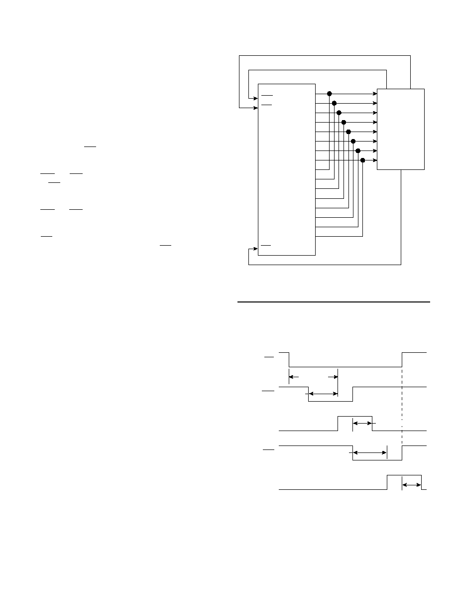
FIGURE 11. 8-BIT DATA TRANSFER
FIGURE 12. 8-BIT DATA TRANSFER TIMING
Note: For further understanding refer to the beginning of this sec-
tion (i.e., Digital Interface, Digital Angle Outputs, Digital Angle
Output Timing, and Inhibit).
DATA TRANSFER TO 16-BIT BUS
Data transfer to the 16-bit bus is much simpler than the 8-bit bus.
FIGURES 13 and 14 show the connections and timing for trans-
ferring data from the SD-14531 to a 16-bit bus.
As can be seen by the timing diagram the following occurs:
1. The converter INH control is applied and must remain low for
a minimum of 500 ns before valid data is transferred.
2. HBE and LBE are set to a low state (logic 0) 350 ns minimum
after INH goes low and must remain low for a minimum of 150 ns
before the data (1-16) is valid and transferred.
3. HBE and LBE should go high (to logic 1) at least 100 ns MAX
before another device uses the bus.
4. INH goes high and data transfer is done and the data refresh
cycle can begin. Note the time it takes for INH to go to a logic 1
should be 100 ns minimum before valid data is transferred.
Note: For further understanding refer to the beginning of this sec-
tion (i.e., Digital Interface, Digital Angle Outputs, Digital Angle
Output Timing, and Inhibit).
INTERFACING - ANALOG OUTPUTS
The analog outputs are AC error (e), Analog Return (V), and
Velocity (VEL).
AC ERROR (e, PIN 12)
The AC error is proportional to the difference between the input
angle
θ and the digital input angle φ, (θ-φ), with a scaling of:
3.5 mV rms/LSB (14-bit mode)
1.75 mV rms/LSB (16-bit mode)
The e output can swing ±3 V min with respect to Analog Return (V).
ANALOG RETURN (V, PIN 11)
This internal voltage is not required externally for normal opera-
tion of the converter. It is used as the internal DC reference and
the return for the VEL and e outputs. It is nominally +4.3 V and is
proportional to the +5 V DC supply.
VELOCITY (VEL, PIN 10)
The velocity output (VEL, pin 10) is a DC voltage proportional to
angular velocity d
θ/dt. The velocity is the input to the voltage-
controlled oscillator (VCO), as shown in FIGURE 1. Its linearity
相關(guān)PDF資料 |
PDF描述 |
|---|---|
| SD-14531F3-885Y | SYNCHRO OR RESOLVER TO DIGITAL CONVERTER, CDMA36 |
| SD-14531F3-885Z | SYNCHRO OR RESOLVER TO DIGITAL CONVERTER, CDMA36 |
| SD-14531F3-892W | SYNCHRO OR RESOLVER TO DIGITAL CONVERTER, CDMA36 |
| SD-14531F3-892Y | SYNCHRO OR RESOLVER TO DIGITAL CONVERTER, CDMA36 |
| SD-14531F3-894Q | SYNCHRO OR RESOLVER TO DIGITAL CONVERTER, CDMA36 |
相關(guān)代理商/技術(shù)參數(shù) |
參數(shù)描述 |
|---|---|
| SD1455 | 功能描述:射頻雙極電源晶體管 NPN 25V 170-230MHz RoHS:否 制造商:M/A-COM Technology Solutions 配置:Single 直流集電極/Base Gain hfe Min:40 最大工作頻率:30 MHz 集電極—發(fā)射極最大電壓 VCEO:25 V 發(fā)射極 - 基極電壓 VEBO:4 V 集電極連續(xù)電流:20 A 最大直流電集電極電流: 功率耗散:250 W 封裝 / 箱體:Case 211-11 封裝:Tray |
| SD1456 | 功能描述:射頻雙極電源晶體管 NPN 28V 170-230MHz RoHS:否 制造商:M/A-COM Technology Solutions 配置:Single 直流集電極/Base Gain hfe Min:40 最大工作頻率:30 MHz 集電極—發(fā)射極最大電壓 VCEO:25 V 發(fā)射極 - 基極電壓 VEBO:4 V 集電極連續(xù)電流:20 A 最大直流電集電極電流: 功率耗散:250 W 封裝 / 箱體:Case 211-11 封裝:Tray |
| SD1457 | 功能描述:射頻放大器 RF Bipolar Trans RoHS:否 制造商:Skyworks Solutions, Inc. 類型:Low Noise Amplifier 工作頻率:2.3 GHz to 2.8 GHz P1dB:18.5 dBm 輸出截獲點(diǎn):37.5 dBm 功率增益類型:32 dB 噪聲系數(shù):0.85 dB 工作電源電壓:5 V 電源電流:125 mA 測試頻率:2.6 GHz 最大工作溫度:+ 85 C 安裝風(fēng)格:SMD/SMT 封裝 / 箱體:QFN-16 封裝:Reel |
| SD1458 | 功能描述:射頻放大器 RF Bipolar Trans RoHS:否 制造商:Skyworks Solutions, Inc. 類型:Low Noise Amplifier 工作頻率:2.3 GHz to 2.8 GHz P1dB:18.5 dBm 輸出截獲點(diǎn):37.5 dBm 功率增益類型:32 dB 噪聲系數(shù):0.85 dB 工作電源電壓:5 V 電源電流:125 mA 測試頻率:2.6 GHz 最大工作溫度:+ 85 C 安裝風(fēng)格:SMD/SMT 封裝 / 箱體:QFN-16 封裝:Reel |
| SD1459 | 功能描述:射頻雙極電源晶體管 NPN 28V 170-230MHz RoHS:否 制造商:M/A-COM Technology Solutions 配置:Single 直流集電極/Base Gain hfe Min:40 最大工作頻率:30 MHz 集電極—發(fā)射極最大電壓 VCEO:25 V 發(fā)射極 - 基極電壓 VEBO:4 V 集電極連續(xù)電流:20 A 最大直流電集電極電流: 功率耗散:250 W 封裝 / 箱體:Case 211-11 封裝:Tray |
發(fā)布緊急采購,3分鐘左右您將得到回復(fù)。