- 您現(xiàn)在的位置:買賣IC網 > PDF目錄376339 > SCAN90CP02SPX (NATIONAL SEMICONDUCTOR CORP) 1.5 Gbps 2x2 LVDS Crosspoint Switch with Pre-Emphasis and IEEE 1149.6 PDF資料下載
參數(shù)資料
| 型號: | SCAN90CP02SPX |
| 廠商: | NATIONAL SEMICONDUCTOR CORP |
| 元件分類: | 運動控制電子 |
| 英文描述: | 1.5 Gbps 2x2 LVDS Crosspoint Switch with Pre-Emphasis and IEEE 1149.6 |
| 中文描述: | 2-CHANNEL, CROSS POINT SWITCH, PQCC28 |
| 封裝: | PLASTIC, LLP-28 |
| 文件頁數(shù): | 7/12頁 |
| 文件大?。?/td> | 261K |
| 代理商: | SCAN90CP02SPX |
Electrical Characteristics
(Continued)
Over recommended operating supply and temperature ranges unless other specified.
Symbol
Parameter
Conditions
Min
Typ
(Note 4)
Max
Units
t
SW
LVDS Switching Time
SELx to OUT
±
Time from configuration select (SELx)
to new switch configuration effective for
OUT
±
.
110
150
ns
SCAN Circuitry Timing Requirements
Symbol
f
MAX
t
S
t
H
t
S
t
H
t
W
t
W
t
REC
Parameter
Maximum TCK Clock Frequency
TDI to TCK, H or L
TDI to TCK, H or L
TMS to TCK, H or L
TMS to TCK, H or L
TCK Pulse Width, H or L
TRST Pulse Width, L
Recovery Time, TRST to TCK
Conditions
R
L
= 500
,
C
L
= 35 pF
Min
25.0
1.0
2.0
2.0
1.5
10.0
2.5
2.0
Typ
Max
Units
MHz
ns
ns
ns
ns
ns
ns
ns
Note 3:
“Absolute Maximum Ratings” are the ratings beyond which the safety of the device cannot be guaranteed. They are not meant to imply that the device
should be operated at these limits.
Note 4:
Typical parameters are measured at V
DD
= 3.3V, T
A
= 25C. They are for reference purposes, and are not production-tested.
Note 5:
Differential output voltage V
OD
is defined as ABS(OUT+–OUT). Differential input voltage V
ID
is defined as ABS(IN+–IN).
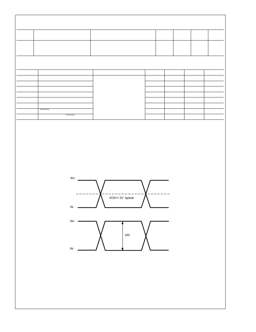
Note 6:
Output offset voltage V
OS
is defined as the average of the LVDS single-ended output voltages at logic high and logic low states.
Note 7:
JIT is the jitter from any input to any one differential LVDS output running at the specified data rate and data pattern, the other channel is powered off. Jitter
is not production tested, but guaranteed through characterization on a sample basis. Random Jitter is measured RMS with a histogram including 1500 histogram
window hits. K28.5 pattern is repeating bit streams of (0011111010 1100000101). This deterministic jitter or DJ pattern is measured to a histogram mean with a
sample size of 350 hits. Total Jitter is measured peak to peak with a histogram including 3500 window hits.
Timing Diagrams
20071415
FIGURE 3. LVDS Signals
S
www.national.com
7
相關PDF資料 |
PDF描述 |
|---|---|
| SCAN90CP02VY | Tape RoHS Compliant: Yes |
| SCAN921023SLC | 20-66 MHz 10 Bit Bus LVDS Serializer and Deserializer |
| SCAN921224 | 20-66 MHz 10 Bit Bus LVDS Serializer and Deserializer |
| SCAN921224SLC | 20-66 MHz 10 Bit Bus LVDS Serializer and Deserializer |
| SCAN921025H | High Temperature 20-80 MHz 10 Bit Bus LVDS SerDes with IEEE 1149.1 (JTAG) and at-speed BIST |
相關代理商/技術參數(shù) |
參數(shù)描述 |
|---|---|
| SCAN90CP02SPX/NOPB | 功能描述:模擬和數(shù)字交叉點 IC RoHS:否 制造商:Micrel 配置:2 x 2 封裝 / 箱體:MLF-16 數(shù)據(jù)速率:10.7 Gbps 輸入電平:CML, LVDS, LVPECL 輸出電平:CML 電源電壓-最大:3.6 V 電源電壓-最小:2.375 V 最大工作溫度:+ 85 C 最小工作溫度:- 40 C 產品:Digital Crosspoint 封裝:Tube |
| SCAN90CP02VY | 功能描述:模擬和數(shù)字交叉點 IC RoHS:否 制造商:Micrel 配置:2 x 2 封裝 / 箱體:MLF-16 數(shù)據(jù)速率:10.7 Gbps 輸入電平:CML, LVDS, LVPECL 輸出電平:CML 電源電壓-最大:3.6 V 電源電壓-最小:2.375 V 最大工作溫度:+ 85 C 最小工作溫度:- 40 C 產品:Digital Crosspoint 封裝:Tube |
| SCAN90CP02VY/NOPB | 功能描述:模擬和數(shù)字交叉點 IC RoHS:否 制造商:Micrel 配置:2 x 2 封裝 / 箱體:MLF-16 數(shù)據(jù)速率:10.7 Gbps 輸入電平:CML, LVDS, LVPECL 輸出電平:CML 電源電壓-最大:3.6 V 電源電壓-最小:2.375 V 最大工作溫度:+ 85 C 最小工作溫度:- 40 C 產品:Digital Crosspoint 封裝:Tube |
| SCAN90CP02VYX | 功能描述:模擬和數(shù)字交叉點 IC RoHS:否 制造商:Micrel 配置:2 x 2 封裝 / 箱體:MLF-16 數(shù)據(jù)速率:10.7 Gbps 輸入電平:CML, LVDS, LVPECL 輸出電平:CML 電源電壓-最大:3.6 V 電源電壓-最小:2.375 V 最大工作溫度:+ 85 C 最小工作溫度:- 40 C 產品:Digital Crosspoint 封裝:Tube |
| SCAN90CP02VYX/NOPB | 功能描述:模擬和數(shù)字交叉點 IC RoHS:否 制造商:Micrel 配置:2 x 2 封裝 / 箱體:MLF-16 數(shù)據(jù)速率:10.7 Gbps 輸入電平:CML, LVDS, LVPECL 輸出電平:CML 電源電壓-最大:3.6 V 電源電壓-最小:2.375 V 最大工作溫度:+ 85 C 最小工作溫度:- 40 C 產品:Digital Crosspoint 封裝:Tube |
發(fā)布緊急采購,3分鐘左右您將得到回復。