- 您現(xiàn)在的位置:買賣IC網 > PDF目錄271769 > SB-36220I1-315 (DATA DEVICE CORP) DIGITAL TO SYNCHRO OR RESOLVER, XMA50 PDF資料下載
參數(shù)資料
| 型號: | SB-36220I1-315 |
| 廠商: | DATA DEVICE CORP |
| 元件分類: | 位置變換器 |
| 英文描述: | DIGITAL TO SYNCHRO OR RESOLVER, XMA50 |
| 文件頁數(shù): | 7/12頁 |
| 文件大小: | 247K |
| 代理商: | SB-36220I1-315 |

4
Data Device Corporation
www.ddc-web.com
SB-36220IX
L-01/06-0
locates a configuration in the system that satisfies the card
requirements. The card communicates with the BIOS to deter-
mine how much memory it requires, along with any other oper-
ating parameters that the system needs to know by way of con-
figuration registers built into the card.
These registers are configured at the factory to contain the opti-
mum values for the operation of the SB-3622X. There is no need
for the user to provide a specific memory location or size, or have
to manipulate interrupts to get the Digital-to-Synchro/Resolver
(D-S/R) card installed. The SB-3622X PCI card and software dri-
vers allow for shared interrupts, thus simplifying the installation
and reducing the risk of device conflicts.
SIGNAL INPUT / OUTPUT CONFIGURATION
Input and output options are created by factory installation of
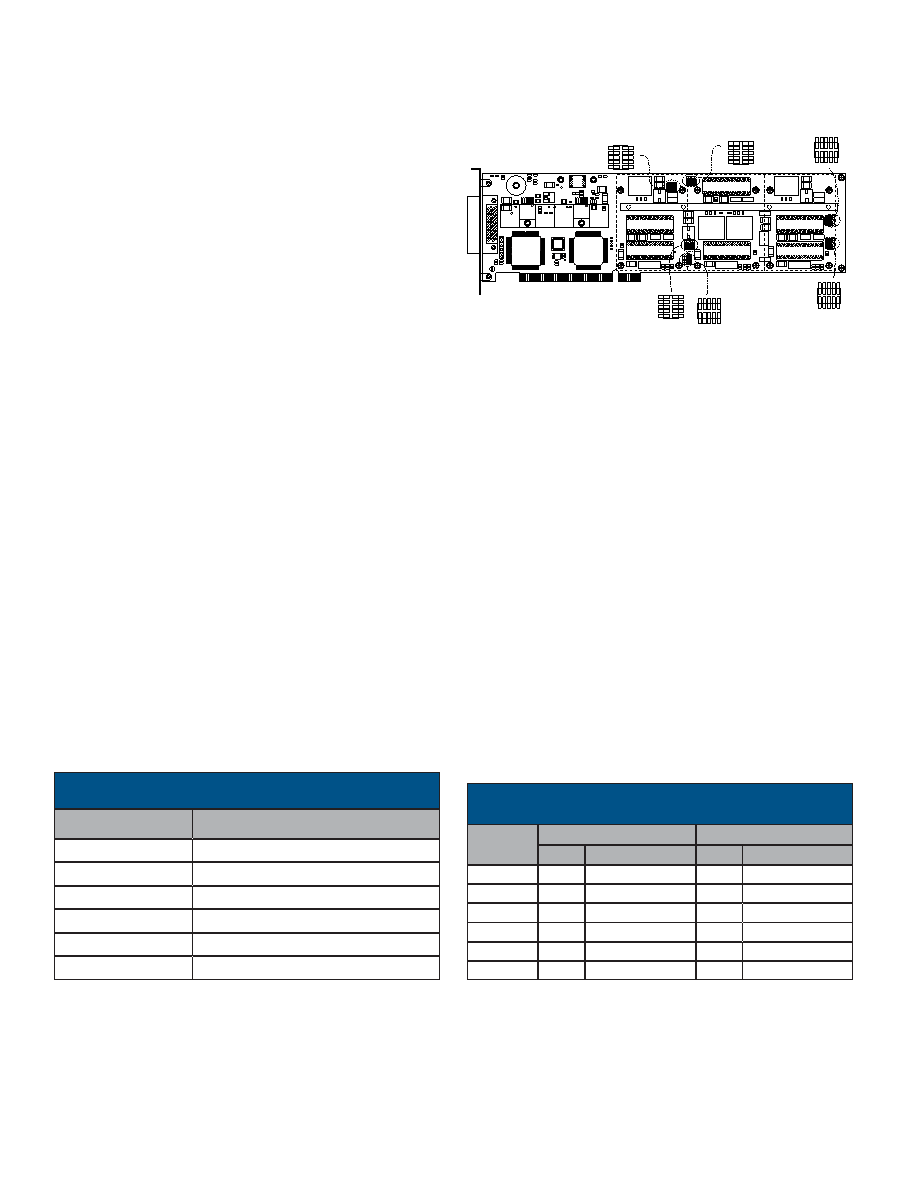
jumpers (TB1 to TB6) on each of the available channels. TABLE 2
lists the Jumper Block designations for each channel. TABLE 3 lists
the “D” connector reference input pins for each channel. TABLE 4
lists the jumper installation for each input option. TABLE 5 lists the
jumper installation for each output option. FIGURE 4 shows the
jumper location and configuration for jumper blocks TB1 to TB6.
Pins 1 through 6 of each TB jumper block (TB1-TB6) determine
the card’s output configuration. Pins 7 through 10 determine the
card’s input configuration.
NOTE: The output signal configuration of the hybrids will match the output type
option selected for types 5 through 8 (see ordering information) which
require a daughter board.
INPUT CONFIGURATION
TBx Jumpers are configured as per Table 4 to select the appro-
priate input option based upon the card’s Reference option (see
ordering information).
U4
U2
U3
U1
U11
T3
1
23
4
5
6
7
8
9
10
2
13
4
5
6
7
8
9
10
1
2
3
4
5
6
7
8
9
10
9
10 8
7
6
5
4
3
2
1
10
9
8
7
6
5
4
3
2
1
10
9
8
7
6
5
4
3
2
1
TB1
TB2
TB4
TB5
TB3
TB6
FIGURE 4. SB-3622X JUMPER LOCATION
TB1
1
TB2
2
TB3
3
TB4
4
TB5
5
TB6
6
JUMPER BLOCK
CHANNEL
TABLE 2. TBx JUMPER BLOCK DESIGNATIONS
TABLE 3. “D” CONNECTOR CHANNEL REFERENCE
INPUT ASSIGNMENTS
1
17
2
24
3
6
4
13
5
8
6
14
CHANNEL
REFERENCE HIGH
19
7
22
9
15
5
REFERENCE LOW
PIN #
FUNCTION
PIN #
FUNCTION
RH_EXT_CH1
RH_EXT_CH2
RH_EXT_CH3
RH_EXT_CH4
RH_EXT_CH5
RH_EXT_CH6
RL_EXT_CH1
RL_EXT_CH2
RL_EXT_CH3
RL_EXT_CH4
RL_EXT_CH5
RL_EXT_CH6
相關PDF資料 |
PDF描述 |
|---|---|
| SD-14597D2-222 | SYNCHRO OR RESOLVER TO DIGITAL CONVERTER, DIP36 |
| SD-14597D2-312 | SYNCHRO OR RESOLVER TO DIGITAL CONVERTER, DIP36 |
| SD-14597F1-315 | SYNCHRO OR RESOLVER TO DIGITAL CONVERTER, CDFP36 |
| SDC-14615-522W | SYNCHRO OR RESOLVER TO DIGITAL CONVERTER, DIP36 |
| SD-14597D1-565 | SYNCHRO OR RESOLVER TO DIGITAL CONVERTER, DIP36 |
相關代理商/技術參數(shù) |
參數(shù)描述 |
|---|---|
| SB36L-A | 制造商:GULFSEMI 制造商全稱:Gulf Semiconductor 功能描述:SURFACE MOUNT SCHOTTKY BARRIER RECTIFIER VOLTAGE: 60V CURRENT: 3.0A |
| SB370 | 制造商:EIC 制造商全稱:EIC discrete Semiconductors 功能描述:SCHOTTKY BARRIER RECTIFIER DIODES |
| SB370_08 | 制造商:DIODES 制造商全稱:Diodes Incorporated 功能描述:3.0A SCHOTTKY BARRIER RECTIFIER |
| SB370-B | 制造商:DIODES 制造商全稱:Diodes Incorporated 功能描述:3.0A SCHOTTKY BARRIER RECTIFIER |
| SB370S | 制造商:EIC 制造商全稱:EIC discrete Semiconductors 功能描述:SCHOTTKY BARRIER RECTIFIER DIODES |
發(fā)布緊急采購,3分鐘左右您將得到回復。