- 您現(xiàn)在的位置:買賣IC網(wǎng) > PDF目錄372105 > SA572 (NXP Semiconductors N.V.) Programmable Analog Compandor(可編程模擬壓縮擴(kuò)展器) PDF資料下載
參數(shù)資料
| 型號: | SA572 |
| 廠商: | NXP Semiconductors N.V. |
| 英文描述: | Programmable Analog Compandor(可編程模擬壓縮擴(kuò)展器) |
| 中文描述: | 可編程模擬Compandor(可編程模擬壓縮擴(kuò)展器) |
| 文件頁數(shù): | 7/12頁 |
| 文件大?。?/td> | 136K |
| 代理商: | SA572 |
Philips Semiconductors
Product specification
SA572
Programmable analog compandor
1998 Nov 03
7
Q8
Q9
Q10
Q17
X2
Q16
X2
10k
D13
Q14
CR
D15
A3
10k
D11
D12
CA
TRACKING
TRIM
I
R1
I
R2
I
Q
=
2I
R2
V+
IR
VIN
R
–
+
SR00699
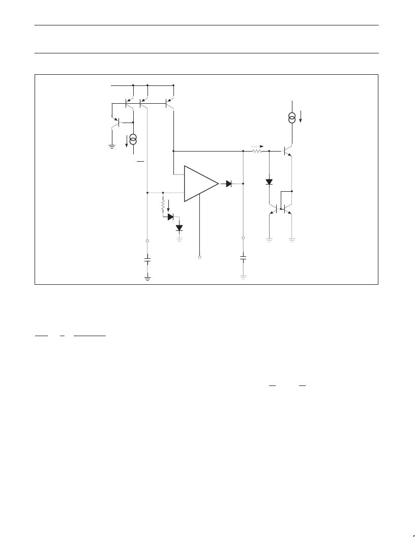
Figure 6. Buffer Amplifier Schematic
Basic Expandor
Figure 7 shows an application of the circuit as a simple expandor.
The gain expression of the system is given by
V
OUT
V
IN
2
I
1
R
3
V
IN(AVG)
R
2
R
1
(5)
(I
1
=140
μ
A)
Both the resistors R
1
and R
2
are tied to internal summing nodes. R
1
is a 6.8k internal resistor. The maximum input current into the gain
cell can be as large as 140
μ
A. This corresponds to a voltage level of
140
μ
A
6.8k=952mV peak. The input peak current into the rectifier
is limited to 300
μ
A by the internal bias system. Note that the value
of R
1
can be increased to accommodate higher input level. R
2
and
R
3
are external resistors. It is easy to adjust the ratio of R
3
/R
2
for
desirable system voltage and current levels. A small R
2
results in
higher gain control current and smaller static and dynamic tracking
error. However, an impedance buffer A
1
may be necessary if the
input is voltage drive with large source impedance.
The gain cell output current feeds the summing node of the external
OPA A
2
. R
3
and A
2
convert the gain cell output current to the output
voltage. In high-performance applications, A
2
has to be low-noise,
high-speed and wide band so that the high-performance output of
the gain cell will not be degraded. The non-inverting input of A
2
can
be biased at the low noise internal reference Pin 6 or 10. Resistor
R
4
is used to bias up the output DC level of A
2
for maximum swing.
The output DC level of A
2
is given by
V
ODC
V
REF
1
R
3
R
4
V
B
R
3
R
4
(6)
V
B
can be tied to a regulated power supply for a dual supply system
and be grounded for a single supply system. CA sets the attack time
constant and CR sets the recovery time constant. *5COL
相關(guān)PDF資料 |
PDF描述 |
|---|---|
| SA5751D | Cell-Phone Circuit |
| SA575AD | Compander |
| SA575ADK | Compander |
| SA575AN | Compander |
| SA575N | Compander |
相關(guān)代理商/技術(shù)參數(shù) |
參數(shù)描述 |
|---|---|
| SA57254-20GW | 制造商:PHILIPS 制造商全稱:NXP Semiconductors 功能描述:CMOS switching regulator (PWM controlled) |
| SA57254-25GW | 制造商:PHILIPS 制造商全稱:NXP Semiconductors 功能描述:CMOS switching regulator (PWM controlled) |
| SA57254-28GW | 制造商:PHILIPS 制造商全稱:NXP Semiconductors 功能描述:CMOS switching regulator (PWM controlled) |
| SA57254-30GW | 制造商:PHILIPS 制造商全稱:NXP Semiconductors 功能描述:CMOS switching regulator (PWM controlled) |
| SA57254-33GW | 制造商:PHILIPS 制造商全稱:NXP Semiconductors 功能描述:CMOS switching regulator (PWM controlled) |
發(fā)布緊急采購,3分鐘左右您將得到回復(fù)。