- 您現(xiàn)在的位置:買賣IC網(wǎng) > PDF目錄192306 > S9705 LOGIC OUTPUT PHOTO DETECTOR PDF資料下載
參數(shù)資料
| 型號: | S9705 |
| 元件分類: | 光電元器件 |
| 英文描述: | LOGIC OUTPUT PHOTO DETECTOR |
| 封裝: | PLASTIC PACKAGE-4 |
| 文件頁數(shù): | 1/2頁 |
| 文件大小: | 0K |
| 代理商: | S9705 |
S9705 is a photo IC that combines a photodiode and a current-to-frequency converter on a CMOS chip. Output is a square wave (50 % duty ratio)
with frequency directly proportional to light intensity incident on the photodiode. The CMOS level digital output allows direct connection to a
microcomputer or other logic circuitry. S9705 has wide dynamic range and light intensity can be easily measured when used with a digital
counter.
Features
l Converts light intensity to frequency
l Wide dynamic range: 5 orders of magnitude
l Excellent linearity
l Output timing reset function
l Digital output for direct interface to microcomputer
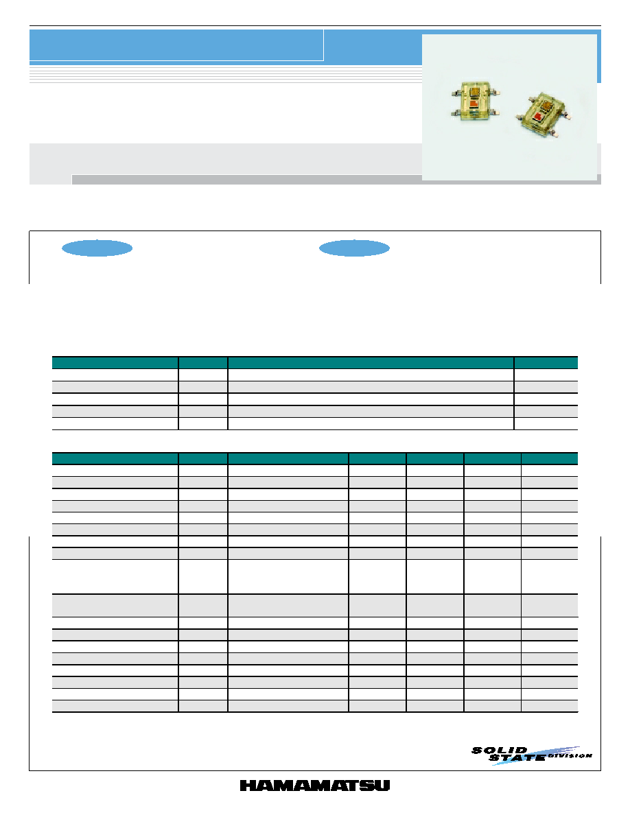
l 4-pin plastic package
Applications
l Liquid crystal monitor backlight dimmer for mobile devices
l Brightness adjustment for large-screen liquid crystal TV
l Lighting dimmer
l Replacement for CdS photoconductive cells
PHOTO
IC
Light-to-frequency converter photo IC
Converts light intensity to frequency of output pulse
S9705
1
s Absolute maximum ratings (Ta=25 °C)
Parameter
Symbol
Value
Unit
Supply voltage
Vdd
-0.3 to 6
V
Load current
Io
±2
mA
Power dissipation
P
50
mW
Operating temperature
Topr
-40 to +85
°C
Storage temperature
Tstg
-40 to +100
°C
s Electrical and optical characteristics (RESET=“L”, Vdd=5 V, Ta=25 °C, unless otherwise noted)
Parameter
Symbol
Condition
Min.
Typ.
Max.
Unit
Peak sensitivity wavelength
λp
-
550
-
nm
Supply voltage
Vdd
2.7
-
5.5
V
Current consumption
Idd
Dark state, no load
-
1.5
3.0
mA
Output frequency
fo
2856 K, 100 lx
38
50
62
kHz
Maximum output frequency
fmax
10 klx, DC light source
300
-
1000
kHz
Response time
tfl
5 lx to 5 mlx, 90 %
-
0.1
s
Dark frequency
fd
0
-
2
Hz
Linearity
-
fo=10 kHz *
1
-3
-
+3
%
Power supply voltage
dependence of output
frequency
-
Vdd=5 V ± 10 %
-
±0.5
-
%/V
Temperature coefficient of
output frequency
-
Ta=25 ± 10 °C, fo=10 kHz
λ=λp
-
±0.02
-
%/°C
Delay time
td
-
0.1
s
High level output voltage
Voh
Ioh= -0.5 mA
4.5
-
V
Low level output voltage
Vol
Iol=0.5 mA
-
0.5
V
Output impedance
Ro
RESET=“H”
1
-
M
High level input voltage
Vih
RESET
4.0
-
V
Low level input voltage
Vil
RESET
-
1.0
V
Input pull-up resistance
Rin
RESET=“L”
0.1
1
5
M
Output pulse duty ratio
D
fo=10 Hz
40
50
60
%
*1: Deviation from the straight line connecting the origin point to the fmax point, normalized by the fmax value.
相關PDF資料 |
PDF描述 |
|---|---|
| SA020-403T | SIP20, IC SOCKET |
| SA030-398G | SIP30, IC SOCKET |
| SA05-11SRWA | 7 SEG NUMERIC DISPLAY, SUPER BRIGHT RED, 12.7 mm |
| SA08-12SURKWA | 7 SEG NUMERIC DISPLAY, HYPER RED, 20.32 mm |
| SA0805175NSTER | ACTIVE DELAY LINE, TRUE OUTPUT, CSIP8 |
相關代理商/技術參數(shù) |
參數(shù)描述 |
|---|---|
| S9706 | 制造商:Hamamatsu Photonics 功能描述: |
| S971 | 制造商:EPCOS 制造商全稱:EPCOS 功能描述:NTC thermistors for temperature measurement |
| S9717 | 制造商:HAMAMATSU 制造商全稱:Hamamatsu Corporation 功能描述:Si APD High reliability, surface-mount ceramic package |
| S9717_11 | 制造商:HAMAMATSU 制造商全稱:Hamamatsu Corporation 功能描述:High reliability, surface-mount ceramic package |
| S9717-02K | 制造商:HAMAMATSU 制造商全稱:Hamamatsu Corporation 功能描述:Si APD High reliability, surface-mount ceramic package |
發(fā)布緊急采購,3分鐘左右您將得到回復。