- 您現(xiàn)在的位置:買賣IC網(wǎng) > PDF目錄373358 > S9703-11 (Hamamatsu Photonics) Photo IC for laser beam synchronous detection PDF資料下載
參數(shù)資料
| 型號(hào): | S9703-11 |
| 廠商: | Hamamatsu Photonics |
| 英文描述: | Photo IC for laser beam synchronous detection |
| 中文描述: | 照片激光束同步檢測(cè)集成電路 |
| 文件頁數(shù): | 2/2頁 |
| 文件大小: | 70K |
| 代理商: | S9703-11 |
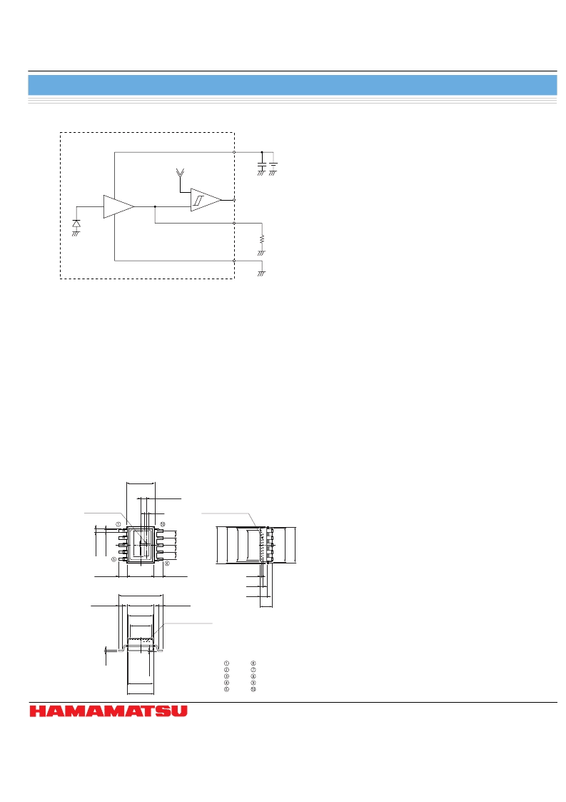
Photo IC for laser beam synchronous detection
S9703-10/-11
HAMAMATSU PHOTONICS K.K., Solid State Division
1126-1 Ichino-cho, Higashi-ku, Hamamatsu City, 435-8558 Japan, Telephone: (81) 53-434-3311, Fax: (81) 53-434-5184, www.hamamatsu.com
U.S.A.: Hamamatsu Corporation: 360 Foothill Road, P.O.Box 6910, Bridgewater, N.J. 08807-0910, U.S.A., Telephone: (1) 908-231-0960, Fax: (1) 908-231-1218
Germany: Hamamatsu Photonics Deutschland GmbH: Arzbergerstr. 10, D-82211 Herrsching am Ammersee, Germany, Telephone: (49) 08152-3750, Fax: (49) 08152-2658
France: Hamamatsu Photonics France S.A.R.L.: 19, Rue du Saule Trapu, Parc du Moulin de Massy, 91882 Massy Cedex, France, Telephone: 33-(1) 69 53 71 00, Fax: 33-(1) 69 53 71 10
United Kingdom: Hamamatsu Photonics UK Limited: 2 Howard Court, 10 Tewin Road, Welwyn Garden City, Hertfordshire AL7 1BW, United Kingdom, Telephone: (44) 1707-294888, Fax: (44) 1707-325777
North Europe: Hamamatsu Photonics Norden AB: Smidesv
gen 12, SE-171 41 Solna, Sweden, Telephone: (46) 8-509-031-00, Fax: (46) 8-509-031-01
Italy: Hamamatsu Photonics Italia S.R.L.: Strada della Moia, 1/E, 20020 Arese, (Milano), Italy, Telephone: (39) 02-935-81-733, Fax: (39) 02-935-81-741
Information furnished by HAMAMATSU is believed to be reliable. However, no responsibility is assumed for possible inaccuracies or omissions.
Specifications are subject to change without notice. No patent rights are granted to any of the circuits described herein. 2007 Hamamatsu Photonics K.K.
Cat. No. KPIC1068E0
2
A
ug
. 2007 DN
2
0.66 ± 0.2
3.2 ± 0.2
(INCLUDING BURR)
3.0 *
1.0 ± 0.4
1.0 ± 0.4
0.05
2.4
MIRRANGE
0
2.8
2.9
3.0 *
0.45 ± 0.3
3.0 *
3
M
R
3
3
4
4
4
5.0 ± 0.3
0.45 ± 0.3
0.35
0.75
1.3
0
0
0
0
0
(
×
)
(
×
)
0.5
PHOTOSENSITIVE
SURFACE
Tolerance unless otherwise noted: ±0.1, ±2
Shaded area indicates burr.
Chip position accuracy with respect to the
package dimensions marked *
X, Y
≤
±0.2,
θ
≤
±2
Vcc
NC
OUT
GND
Ro
GND
GND
GND
GND
GND
0
2
CENTER OF
ACTIVE AREA
PHOTOSENSITIVE
SURFACE
I
Dimensional outline (unit: mm)
KPICC0113EA
I
Block diagram
Vcc
0.1
μ
F
5 V
CURRENT
AMPLIFIER
EXTERNAL
GAIN RESISTANCE
Ro
Vo
Ro
PD
Vref
GND
I
Function
S9703-10/-11 photo IC integrates a photodiode chip and an IC chip into the same package. The photodiode chip is internally
connected to the IC chip as shown in the block diagram. S9703-10/-11 should be used with terminal Ro connected to an external
gain resistance Ro.
A photocurrent is generated when a laser beam enters the photodiode. This photocurrent is fed to the input terminal of the IC and,
after being amplified by the current amplifier, flows to the external gain resistance. At this time, voltages V
RO
at terminal Ro is
given by the following expression.
V
RO
=A × S × P
I
× Ro [V] ·········· (1)
A: Current amplifier gain (S9703-10: 20 times, S9703-11: 6 times)
S: Photodiode sensitivity [A/W] (approx. 0.44 A/W at 780 nm)
P
I
: Input power [W]
Ro: External gain resistance [
]; usable range 2 k
to 10 k
V
RO
is input to the internal comparator and compared with the internal reference voltage Vref (approx. 1 V) so the output Vo is
“High” when V
RO
< Vref or “Low” when V
RO
> Vref.
In equation (1), set the Ro value so that V
RO
is 2 to 3 V.
KPICA0071EA
相關(guān)PDF資料 |
PDF描述 |
|---|---|
| S9703 | Photo IC for laser beam synchronous detection High sensitivity, high-speed response |
| S9703-01 | Photo IC for laser beam synchronous detection High sensitivity, high-speed response |
| S9706 | Digital color sensor 12-bit digital output |
| S9717 | Si APD High reliability, surface-mount ceramic package |
| S9717-02K | Si APD High reliability, surface-mount ceramic package |
相關(guān)代理商/技術(shù)參數(shù) |
參數(shù)描述 |
|---|---|
| S9706 | 制造商:Hamamatsu Photonics 功能描述: |
| S971 | 制造商:EPCOS 制造商全稱:EPCOS 功能描述:NTC thermistors for temperature measurement |
| S9717 | 制造商:HAMAMATSU 制造商全稱:Hamamatsu Corporation 功能描述:Si APD High reliability, surface-mount ceramic package |
| S9717_11 | 制造商:HAMAMATSU 制造商全稱:Hamamatsu Corporation 功能描述:High reliability, surface-mount ceramic package |
| S9717-02K | 制造商:HAMAMATSU 制造商全稱:Hamamatsu Corporation 功能描述:Si APD High reliability, surface-mount ceramic package |
發(fā)布緊急采購,3分鐘左右您將得到回復(fù)。