- 您現(xiàn)在的位置:買賣IC網(wǎng) > PDF目錄25641 > S80C32E-20R (ATMEL CORP) 8-BIT, 20 MHz, MICROCONTROLLER, PQCC44 PDF資料下載
參數(shù)資料
| 型號(hào): | S80C32E-20R |
| 廠商: | ATMEL CORP |
| 元件分類: | 微控制器/微處理器 |
| 英文描述: | 8-BIT, 20 MHz, MICROCONTROLLER, PQCC44 |
| 封裝: | PLASTIC, LCC-44 |
| 文件頁(yè)數(shù): | 155/364頁(yè) |
| 文件大小: | 5293K |
| 代理商: | S80C32E-20R |
第1頁(yè)第2頁(yè)第3頁(yè)第4頁(yè)第5頁(yè)第6頁(yè)第7頁(yè)第8頁(yè)第9頁(yè)第10頁(yè)第11頁(yè)第12頁(yè)第13頁(yè)第14頁(yè)第15頁(yè)第16頁(yè)第17頁(yè)第18頁(yè)第19頁(yè)第20頁(yè)第21頁(yè)第22頁(yè)第23頁(yè)第24頁(yè)第25頁(yè)第26頁(yè)第27頁(yè)第28頁(yè)第29頁(yè)第30頁(yè)第31頁(yè)第32頁(yè)第33頁(yè)第34頁(yè)第35頁(yè)第36頁(yè)第37頁(yè)第38頁(yè)第39頁(yè)第40頁(yè)第41頁(yè)第42頁(yè)第43頁(yè)第44頁(yè)第45頁(yè)第46頁(yè)第47頁(yè)第48頁(yè)第49頁(yè)第50頁(yè)第51頁(yè)第52頁(yè)第53頁(yè)第54頁(yè)第55頁(yè)第56頁(yè)第57頁(yè)第58頁(yè)第59頁(yè)第60頁(yè)第61頁(yè)第62頁(yè)第63頁(yè)第64頁(yè)第65頁(yè)第66頁(yè)第67頁(yè)第68頁(yè)第69頁(yè)第70頁(yè)第71頁(yè)第72頁(yè)第73頁(yè)第74頁(yè)第75頁(yè)第76頁(yè)第77頁(yè)第78頁(yè)第79頁(yè)第80頁(yè)第81頁(yè)第82頁(yè)第83頁(yè)第84頁(yè)第85頁(yè)第86頁(yè)第87頁(yè)第88頁(yè)第89頁(yè)第90頁(yè)第91頁(yè)第92頁(yè)第93頁(yè)第94頁(yè)第95頁(yè)第96頁(yè)第97頁(yè)第98頁(yè)第99頁(yè)第100頁(yè)第101頁(yè)第102頁(yè)第103頁(yè)第104頁(yè)第105頁(yè)第106頁(yè)第107頁(yè)第108頁(yè)第109頁(yè)第110頁(yè)第111頁(yè)第112頁(yè)第113頁(yè)第114頁(yè)第115頁(yè)第116頁(yè)第117頁(yè)第118頁(yè)第119頁(yè)第120頁(yè)第121頁(yè)第122頁(yè)第123頁(yè)第124頁(yè)第125頁(yè)第126頁(yè)第127頁(yè)第128頁(yè)第129頁(yè)第130頁(yè)第131頁(yè)第132頁(yè)第133頁(yè)第134頁(yè)第135頁(yè)第136頁(yè)第137頁(yè)第138頁(yè)第139頁(yè)第140頁(yè)第141頁(yè)第142頁(yè)第143頁(yè)第144頁(yè)第145頁(yè)第146頁(yè)第147頁(yè)第148頁(yè)第149頁(yè)第150頁(yè)第151頁(yè)第152頁(yè)第153頁(yè)第154頁(yè)當(dāng)前第155頁(yè)第156頁(yè)第157頁(yè)第158頁(yè)第159頁(yè)第160頁(yè)第161頁(yè)第162頁(yè)第163頁(yè)第164頁(yè)第165頁(yè)第166頁(yè)第167頁(yè)第168頁(yè)第169頁(yè)第170頁(yè)第171頁(yè)第172頁(yè)第173頁(yè)第174頁(yè)第175頁(yè)第176頁(yè)第177頁(yè)第178頁(yè)第179頁(yè)第180頁(yè)第181頁(yè)第182頁(yè)第183頁(yè)第184頁(yè)第185頁(yè)第186頁(yè)第187頁(yè)第188頁(yè)第189頁(yè)第190頁(yè)第191頁(yè)第192頁(yè)第193頁(yè)第194頁(yè)第195頁(yè)第196頁(yè)第197頁(yè)第198頁(yè)第199頁(yè)第200頁(yè)第201頁(yè)第202頁(yè)第203頁(yè)第204頁(yè)第205頁(yè)第206頁(yè)第207頁(yè)第208頁(yè)第209頁(yè)第210頁(yè)第211頁(yè)第212頁(yè)第213頁(yè)第214頁(yè)第215頁(yè)第216頁(yè)第217頁(yè)第218頁(yè)第219頁(yè)第220頁(yè)第221頁(yè)第222頁(yè)第223頁(yè)第224頁(yè)第225頁(yè)第226頁(yè)第227頁(yè)第228頁(yè)第229頁(yè)第230頁(yè)第231頁(yè)第232頁(yè)第233頁(yè)第234頁(yè)第235頁(yè)第236頁(yè)第237頁(yè)第238頁(yè)第239頁(yè)第240頁(yè)第241頁(yè)第242頁(yè)第243頁(yè)第244頁(yè)第245頁(yè)第246頁(yè)第247頁(yè)第248頁(yè)第249頁(yè)第250頁(yè)第251頁(yè)第252頁(yè)第253頁(yè)第254頁(yè)第255頁(yè)第256頁(yè)第257頁(yè)第258頁(yè)第259頁(yè)第260頁(yè)第261頁(yè)第262頁(yè)第263頁(yè)第264頁(yè)第265頁(yè)第266頁(yè)第267頁(yè)第268頁(yè)第269頁(yè)第270頁(yè)第271頁(yè)第272頁(yè)第273頁(yè)第274頁(yè)第275頁(yè)第276頁(yè)第277頁(yè)第278頁(yè)第279頁(yè)第280頁(yè)第281頁(yè)第282頁(yè)第283頁(yè)第284頁(yè)第285頁(yè)第286頁(yè)第287頁(yè)第288頁(yè)第289頁(yè)第290頁(yè)第291頁(yè)第292頁(yè)第293頁(yè)第294頁(yè)第295頁(yè)第296頁(yè)第297頁(yè)第298頁(yè)第299頁(yè)第300頁(yè)第301頁(yè)第302頁(yè)第303頁(yè)第304頁(yè)第305頁(yè)第306頁(yè)第307頁(yè)第308頁(yè)第309頁(yè)第310頁(yè)第311頁(yè)第312頁(yè)第313頁(yè)第314頁(yè)第315頁(yè)第316頁(yè)第317頁(yè)第318頁(yè)第319頁(yè)第320頁(yè)第321頁(yè)第322頁(yè)第323頁(yè)第324頁(yè)第325頁(yè)第326頁(yè)第327頁(yè)第328頁(yè)第329頁(yè)第330頁(yè)第331頁(yè)第332頁(yè)第333頁(yè)第334頁(yè)第335頁(yè)第336頁(yè)第337頁(yè)第338頁(yè)第339頁(yè)第340頁(yè)第341頁(yè)第342頁(yè)第343頁(yè)第344頁(yè)第345頁(yè)第346頁(yè)第347頁(yè)第348頁(yè)第349頁(yè)第350頁(yè)第351頁(yè)第352頁(yè)第353頁(yè)第354頁(yè)第355頁(yè)第356頁(yè)第357頁(yè)第358頁(yè)第359頁(yè)第360頁(yè)第361頁(yè)第362頁(yè)第363頁(yè)第364頁(yè)
238
8023F–AVR–07/09
ATmega325P/3250P
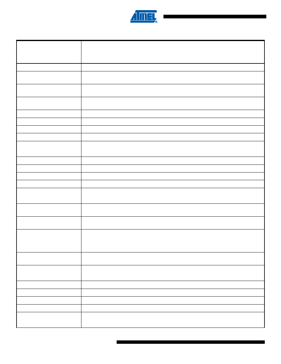
Table 23-4.
Boundary-scan Signals for the ADC
Signal
Name
Direction as
seen
from the ADC
Description
Recommende
d Input when
not in use
Output Values when
recommended inputs are
used, and CPU is not using the
ADC
COMP
Output
Comparator Output
0
ACLK
Input
Clock signal to differential amplifier
implemented as Switch-cap filters
00
ACTEN
Input
Enable path from differential amplifier to
the comparator
00
ADCBGEN
Input
Enable Band-gap reference as negative
input to comparator
00
ADCEN
Input
Power-on signal to the ADC
0
AMPEN
Input
Power-on signal to the differential amplifier
0
DAC_9
Input
Bit 9 of digital value to DAC
1
DAC_8
Input
Bit 8 of digital value to DAC
0
DAC_7
Input
Bit 7 of digital value to DAC
0
DAC_6
Input
Bit 6 of digital value to DAC
0
DAC_5
Input
Bit 5 of digital value to DAC
0
DAC_4
Input
Bit 4 of digital value to DAC
0
DAC_3
Input
Bit 3 of digital value to DAC
0
DAC_2
Input
Bit 2 of digital value to DAC
0
DAC_1
Input
Bit 1 of digital value to DAC
0
DAC_0
Input
Bit 0 of digital value to DAC
0
EXTCH
Input
Connect ADC channels 0 - 3 to by-pass
path around differential amplifier
11
GNDEN
Input
Ground the negative input to comparator
when true
00
HOLD
Input
Sample & Hold signal. Sample analog
signal when low. Hold signal when high. If
differential amplifier are used, this signal
must go active when ACLK is high.
11
IREFEN
Input
Enables Band-gap reference as AREF
signal to DAC
00
MUXEN_7
Input
Input Mux bit 7
0
MUXEN_6
Input
Input Mux bit 6
0
MUXEN_5
Input
Input Mux bit 5
0
MUXEN_4
Input
Input Mux bit 4
0
MUXEN_3
Input
Input Mux bit 3
0
MUXEN_2
Input
Input Mux bit 2
0
MUXEN_1
Input
Input Mux bit 1
0
MUXEN_0
Input
Input Mux bit 0
1
相關(guān)PDF資料 |
PDF描述 |
|---|---|
| MQ83C154CXXX-12P883R | 8-BIT, MROM, 12 MHz, MICROCONTROLLER, CQFP44 |
| MC80C52EXXX-25SHXXX | 8-BIT, MROM, 25 MHz, MICROCONTROLLER, CDIP40 |
| MC80C52XXX-30/883:D | 8-BIT, MROM, 30 MHz, MICROCONTROLLER, CDIP40 |
| S83C154DXXX-25R | 8-BIT, MROM, 25 MHz, MICROCONTROLLER, PQCC44 |
| S80C52CXXX-16D | 8-BIT, MROM, 16 MHz, MICROCONTROLLER, PQCC44 |
相關(guān)代理商/技術(shù)參數(shù) |
參數(shù)描述 |
|---|---|
| S80C32-L16 | 制造商:未知廠家 制造商全稱:未知廠家 功能描述:8-Bit Microcontroller |
| S80C32-L16R | 制造商:未知廠家 制造商全稱:未知廠家 功能描述:8-Bit Microcontroller |
| S80C376CB8 WAF | 制造商:Intel 功能描述: |
| S80C42 | 制造商:Intel 功能描述: |
| S80C51 WAF | 制造商:Intel 功能描述: |
發(fā)布緊急采購(gòu),3分鐘左右您將得到回復(fù)。