- 您現(xiàn)在的位置:買賣IC網(wǎng) > PDF目錄26854 > S7141-10 LOGIC OUTPUT PHOTO DETECTOR PDF資料下載
參數(shù)資料
| 型號(hào): | S7141-10 |
| 元件分類: | 光電元器件 |
| 英文描述: | LOGIC OUTPUT PHOTO DETECTOR |
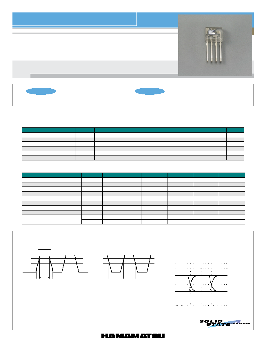
| 封裝: | PLASTIC PACKAGE-4 |
| 文件頁(yè)數(shù): | 1/2頁(yè) |
| 文件大小: | 70K |
| 代理商: | S7141-10 |
PHOTO
IC
Photo IC for optical link
Photo IC for 50 Mbps optical link
S7141-10
Features
l DC to 50 Mbps data transmission
l Miniature size due to monolithic IC structure
l Inversion logic
l Digital output
l Designed to be used with L8045
Applications
l Data transmission in FA or OA applications subject to large
amounts of electro magnetic noise
l High-speed, short distance data transmission
l Burst data transmission
1
1.8 V
1.5 V
1.2 V
tr
tf
pw
T = pw1 - pw
s Input optical waveform definition
pw1
tr=2 ns
tf=5 ns
80 %
50 %
20 %
s Output optical waveform definition
5 ns/div.
KPICC0023EB
KPICC0022EA
s S7141-10 output waveform example
(Input light is referenced by drive circuit
on front page)
(Ta=25 °C, Pi= -16 dBm, Vcc=5.0 V)
KPICC0068EA
s Electrical and optical characteristics (Ta=25
°C)
Parameter
Symbol
Condition
Min.
Typ.
Max.
Unit
Data rate
fD
DC
50
Mbps
Supply voltage
Vcc
4.75
-
5.25
V
Current consumption
Icc
W ithout light input
-
32
mA
Pulse width distortion
T
-6
-
+6
ns
Minimum overload
Pimax
*
2, *3
-5
-
dBm
Minimum receiver input power
Pimin
*
2, *3
-
-17.5
dBm
Rise time
tr
*
3
--
7
ns
Fall time
tf
*
3
-
7
ns
Voh
Ioh=20 A
2
-
V
Output voltage
Vol
Iol= -0.6 mA *
4
--
1
V
*2: Output from a 1 meter long plastic fiber (GH4001 made by Mitsubishi Rayon) set close to the molded lens.
*3: Evaluated based on the input/output waveforms shown below. Measured with a low-capacitance FET probe (3 pF or less).
*4: Output is the “L” level (inversion logic) when light is input.
s Absolute maximum ratings (Ta=25
°C)
Parameter
Symbol
Value
Unit
Power supply
Vcc
-0.5 to +7
V
Output current
Ioh
10
mA
Power dissipation *
1
P
250
mW
Operating temperature
Topr
-10 to +70
°C
Storage temperature
Tstg
-40 to +85
°C
Soldering
-
230 °C, 5 s, at least 1.5 mm away from package surface
-
*1: Derate power dissipation at a rate of 1.75 mW /°C above Ta=25 °C
相關(guān)PDF資料 |
PDF描述 |
|---|---|
| S7478-01 | PIN PHOTO DIODE |
| S75DC150 | TRANSISTOR OUTPUT SOLID STATE RELAY, 4000 V ISOLATION-MAX |
| S7762 | PIN PHOTO DIODE |
| S8314 | PIN PHOTO DIODE |
| S8041 | LOGIC OUTPUT PHOTO DETECTOR |
相關(guān)代理商/技術(shù)參數(shù) |
參數(shù)描述 |
|---|---|
| S7141-45R | 功能描述:RFI SHIELD FINGER AU 2.5MM SMD 制造商:harwin inc. 系列:- 零件狀態(tài):有效 形狀:- 厚度 - 總:0.098"(2.50mm) 寬度:0.091"(2.30mm) 長(zhǎng)度:0.181"(4.60mm) 粘合劑:- 溫度范圍:-4°F ~ 158°F(-20°C ~ 70°C) 標(biāo)準(zhǔn)包裝:1 |
| S7142 | 制造商:AUK 制造商全稱:AUK corp 功能描述:Bipolar Linear Integrated Circuit |
| S7142AM | 制造商:AUK 制造商全稱:AUK corp 功能描述:Bipolar Linear Integrated Circuit |
| S7142F | 制造商:AUK 制造商全稱:AUK corp 功能描述:Standard Voltage Detector |
| S7142LSF | 制造商:AUK 制造商全稱:AUK corp 功能描述:Bipolar Linear Integrated Circuit |
發(fā)布緊急采購(gòu),3分鐘左右您將得到回復(fù)。