- 您現(xiàn)在的位置:買賣IC網(wǎng) > PDF目錄98011 > S568013MFA00E (FREESCALE SEMICONDUCTOR INC) 0-BIT, 8 MHz, OTHER DSP, PQFP32 PDF資料下載
參數(shù)資料
| 型號: | S568013MFA00E |
| 廠商: | FREESCALE SEMICONDUCTOR INC |
| 元件分類: | 數(shù)字信號處理 |
| 英文描述: | 0-BIT, 8 MHz, OTHER DSP, PQFP32 |
| 封裝: | ROHS COMPLIANT, LQFP-32 |
| 文件頁數(shù): | 96/125頁 |
| 文件大?。?/td> | 1702K |
| 代理商: | S568013MFA00E |
第1頁第2頁第3頁第4頁第5頁第6頁第7頁第8頁第9頁第10頁第11頁第12頁第13頁第14頁第15頁第16頁第17頁第18頁第19頁第20頁第21頁第22頁第23頁第24頁第25頁第26頁第27頁第28頁第29頁第30頁第31頁第32頁第33頁第34頁第35頁第36頁第37頁第38頁第39頁第40頁第41頁第42頁第43頁第44頁第45頁第46頁第47頁第48頁第49頁第50頁第51頁第52頁第53頁第54頁第55頁第56頁第57頁第58頁第59頁第60頁第61頁第62頁第63頁第64頁第65頁第66頁第67頁第68頁第69頁第70頁第71頁第72頁第73頁第74頁第75頁第76頁第77頁第78頁第79頁第80頁第81頁第82頁第83頁第84頁第85頁第86頁第87頁第88頁第89頁第90頁第91頁第92頁第93頁第94頁第95頁當前第96頁第97頁第98頁第99頁第100頁第101頁第102頁第103頁第104頁第105頁第106頁第107頁第108頁第109頁第110頁第111頁第112頁第113頁第114頁第115頁第116頁第117頁第118頁第119頁第120頁第121頁第122頁第123頁第124頁第125頁
56F8013/56F8011 Data Sheet, Rev. 11
72
Freescale Semiconductor
generation and SIM modules. All functionality is for test purposes only and is subject to
unspecified latencies. Glitches may be produced when the clock is enabled or switched.
The lower four bits of the GPIO A register can function as GPIO, PWM, or as additional clock output
signals. GPIO has priority and is enabled/disabled via the GPIOA_PEREN. If GPIOA[3:0] are
programmed to operate as peripheral outputs, then the choice between PWM and additional clock outputs
is done here in the CLKOUT. The default state is for the peripheral function of GPIOA[3:0] to be
programmed as PWM. This can be changed by altering PWM3 through PWM0.
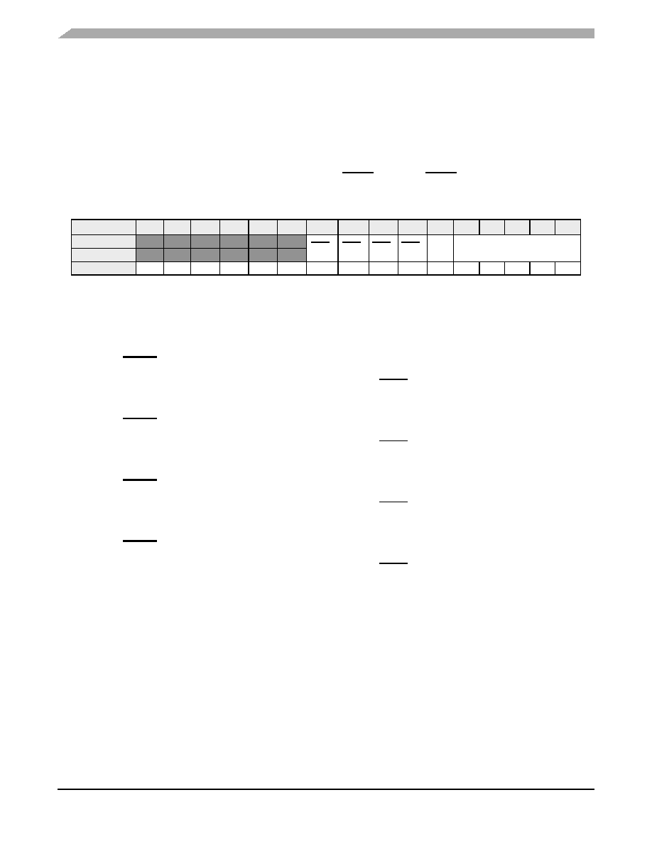
Figure 6-8 CLKO Select Register (SIM_CLKOUT)
6.3.7.1
Reserved—Bits 15–10
This bit field is reserved or not implemented. It is read as 0 and cannot be modified by writing.
6.3.7.2
PWM3—Bit 9
0 = Peripheral output function of GPIOA[3] is defined to be PWM3
1 = Peripheral output function of GPIOA[3] is defined to be the Relaxation Oscillator Clock
6.3.7.3
PWM2—Bit 8
0 = Peripheral output function of GPIOA[2] is defined to be PWM2
1 = Peripheral output function of GPIOA[2] is defined to be the system clock
6.3.7.4
PWM1—Bit 7
0 = Peripheral output function of GPIOA[1] is defined to be PWM1
1 = Peripheral output function of GPIOA[1] is defined to be two times the rate of the system clock
6.3.7.5
PWM0—Bit 6
0 = Peripheral output function of GPIOA[0] is defined to be PWM0
1 = Peripheral output function of GPIOA[0] is defined to be three times the rate of the system clock
6.3.7.6
Clockout Disable (CLKDIS)—Bit 5
0 = CLKOUT output is enabled and will output the signal indicated by CLKOSEL
1 = CLKOUT is 0
6.3.7.7
Clockout Select (CLKOSEL)—Bits 4–0
Selects clock to be muxed out on the CLKO pin.
00000 = Reserved for factory test—Continuous system clock
Base + $A
15
14
13
12
11
10
9
8
7
6
5
4
3
2
1
0
Read
0
PWM3PWM2PWM1PWM0
CLK
DIS
CLKOSEL
Write
RESET
0
1
0
0000
相關(guān)PDF資料 |
PDF描述 |
|---|---|
| MC56F8023VLC | 16-BIT, FLASH, 32 MHz, MICROCONTROLLER, PQFP32 |
| MC56F8033VLC | 16-BIT, FLASH, 32 MHz, MICROCONTROLLER, PQFP32 |
| MC56F8347MPY60 | 16-BIT, 120 MHz, OTHER DSP, PQFP160 |
| MC56F8355VFG60 | 4-BIT, 120 MHz, OTHER DSP, PQFP128 |
| MC56F8355MFG60 | 4-BIT, 120 MHz, OTHER DSP, PQFP128 |
相關(guān)代理商/技術(shù)參數(shù) |
參數(shù)描述 |
|---|---|
| S5-680RF1 | 制造商:Riedon 功能描述:RES 680 OHM 4W 1% WW SMD |
| S5688B | 制造商:TOSHIBA 制造商全稱:Toshiba Semiconductor 功能描述:TOSHIBA Rectifier Silicon Diffused Type |
| S5688B(Q) | 制造商:Toshiba 功能描述:Diode 100V 1A 2-Pin DO-41SS |
| S5688B(TPA2) | 制造商:Toshiba America Electronic Components 功能描述:Diode 100V 1A 2-Pin DO-41SS T/R Cut Tape |
| S5688G | 制造商:Toshiba America Electronic Components 功能描述: 制造商:Panasonic Industrial Company 功能描述:DIODE |
發(fā)布緊急采購,3分鐘左右您將得到回復。