- 您現(xiàn)在的位置:買賣IC網(wǎng) > PDF目錄373348 > S39421 (Electronic Theatre Controls, Inc.) Hot Swap Voltage Controller PDF資料下載
參數(shù)資料
| 型號(hào): | S39421 |
| 廠商: | Electronic Theatre Controls, Inc. |
| 英文描述: | Hot Swap Voltage Controller |
| 中文描述: | 電壓熱插拔控制器 |
| 文件頁(yè)數(shù): | 23/28頁(yè) |
| 文件大小: | 201K |
| 代理商: | S39421 |
第1頁(yè)第2頁(yè)第3頁(yè)第4頁(yè)第5頁(yè)第6頁(yè)第7頁(yè)第8頁(yè)第9頁(yè)第10頁(yè)第11頁(yè)第12頁(yè)第13頁(yè)第14頁(yè)第15頁(yè)第16頁(yè)第17頁(yè)第18頁(yè)第19頁(yè)第20頁(yè)第21頁(yè)第22頁(yè)當(dāng)前第23頁(yè)第24頁(yè)第25頁(yè)第26頁(yè)第27頁(yè)第28頁(yè)
S39421
23
2024 9.0 8/8/00
The S39421 will now begin monitoring the backend circuit
voltages and when they are at or above Vtrip the reset
timer will be released to begin the time out period and
CARD_V_VLD will be released. After tPURST has ex-
pired, the reset outputs will be released and SGNL_VLD
will be driven active. The SGNL_VLD signal can be tied to
the host LI/O* signal pin to indicate the card has been fully
powered, cleanly reset and is ready for action.
Backplane/Add-in Card Sequencing
A more complicated problem than the sequencing shown
above is the signal bus interface. Inserting unpowered
circuits onto the signal bus could lead to a situation of
damaging components and much more likely disrupting
the signals on the backplane. This will involve a rigorous
evaluation and selection process by the design engineer
to determine the best solution for the individual applica-
tion. However, we can examine a product family that
should resolve most of the issues the designer might
encounter. The proposed VME Live Insertion spec actu-
ally helps us narrow this down quickly by recommending
the use of ABTE logic. This is available from at least two
large manufacturers of semiconductors.
Avoidance of Bus Conflicts
Bus conflicts arise when two or more interface circuits
attempt to drive the bus simultaneously with one circuit
driving high and the other driving low. The device trying to
drive low will most likely not incur damage. But the device
trying to drive high will be dropping 5Volts on its output at
up to 120mA current. Even for very short periods of time
the high temperatures this will generate can either destroy
the device or adversely affect the long-term reliability of
the device. The best solution is to insure the transceiver
’
s
enable input is actively driven before the transceiver is
powered-on. Using one of the reset outputs (as shown in
figure 27) as a gating signal to a single enable input style
transceiver is one solution. With a dual enable transceiver
one of the reset outputs can be tied directly to appropriate
enable input.
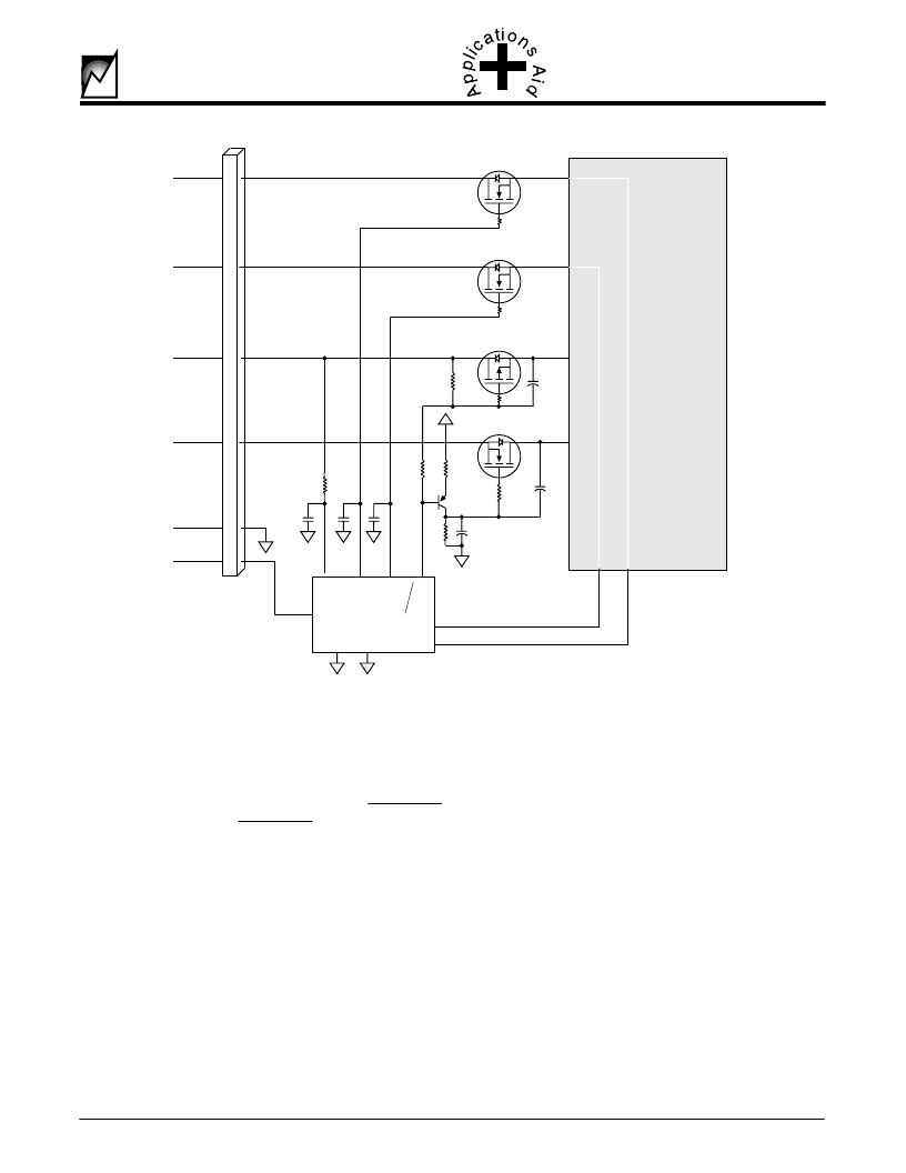
FIGURE 26: BACKEND VOLTAGE CONTROL CIRCUIT
-12V
+12V
+3.3V
+5V
Gnd
Vpc
Gnd
Vpc
VCC5
VC
VT
VAE
S39421
DR
IE
CARD_3V
CARD_5V
VL
B
+5V
+3.3V
-12V
+12V
2024 ILL29.3
相關(guān)PDF資料 |
PDF描述 |
|---|---|
| S39421S | Hot Swap Voltage Controller |
| S3954 | 76-element Si photodiode array High UV sensitivity photodiode array mounted in DIP |
| S3994-01 | Si PIN photodiode for optical power meters |
| S3AB | 3.0A SURFACE MOUNT GLASS PASSVATED RECTIFIER |
| S3MB | 3.0A FAST RECOVERY GLASS PASSIVATED RECTIFIER |
相關(guān)代理商/技術(shù)參數(shù) |
參數(shù)描述 |
|---|---|
| S39421S | 制造商:SUMMIT 制造商全稱:SUMMIT 功能描述:Hot Swap Voltage Controller |
| S394-90-108-00-760000 | 制造商:Mill-Max Mfg Corp 功能描述:Custom Socket |
| S3950G2NR | 制造商:TYAN 功能描述:1P/AMD,(2)LAN,PCI-X,(4)PCI,ATX - Trays |
| S3950G2NR RPL | 制造商:TYAN 功能描述:REPAIR/REPLACEMENT - Bulk |
| S3950G2NR-DF | 制造商:TYAN 功能描述:TYAN TOMCAT H1000S - Bulk |
發(fā)布緊急采購(gòu),3分鐘左右您將得到回復(fù)。