- 您現(xiàn)在的位置:買賣IC網(wǎng) > PDF目錄373328 > RT9209 Step-down DC/DC Converter PDF資料下載
參數(shù)資料
| 型號: | RT9209 |
| 英文描述: | Step-down DC/DC Converter |
| 中文描述: | 降壓直流/直流轉(zhuǎn)換器 |
| 文件頁數(shù): | 5/16頁 |
| 文件大小: | 315K |
| 代理商: | RT9209 |
Preliminary
RT9203/A
DS9203/A-04 May 2003
www.richtek.com
5
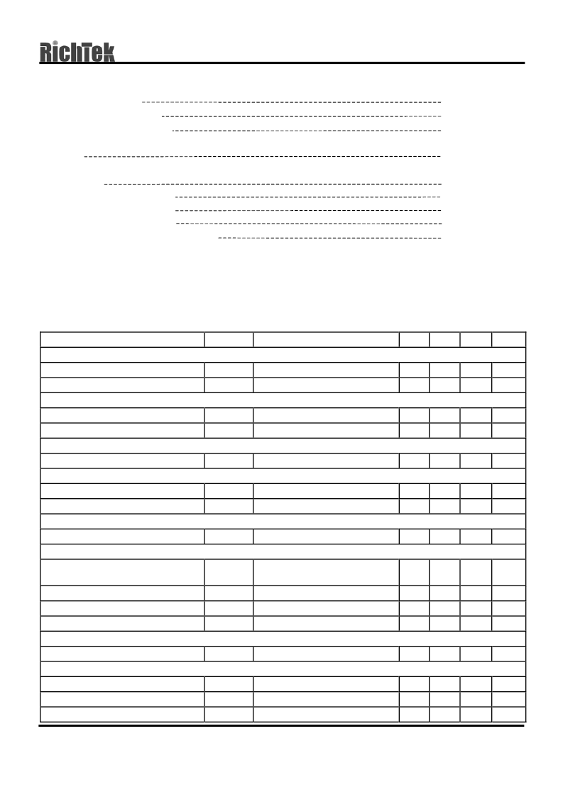
Absolute Maximum Ratings
z
Supply Voltage VCC
7V
19V
GND
0.3V ~ 7V
z
BOOT & UGATE to GND
z
Input, Output or I/O Voltage
z
Power Dissipation, P
D
@ T
A
= 25
°
C
SOP-8
z
Package Thermal Resistance
SOP-8,
θ
JA
z
Ambient Temperature Range
z
Junction Temperature Range
z
Storage Temperature Range
0.625W
160
°
C/W
0
°
C ~ +70
°
C
-40
°
C ~ +125
°
C
-65
°
C ~ +150
°
C
260
°
C
z
Lead Temperature (Soldering, 10 sec.)
CAUTION:
Stresses beyond the ratings specified in “Absolute Maximum Ratings” may cause permanent damage to the device.
This is a stress only rating and operation of the device at these or any other conditions above those indicated in the
operational sections of this specification is not implied.
Electrical Characteristics
(V
CC
= 5V, T
A
= 25
°
C, Unless otherwise specified.)
Parameter
VCC Supply Current
Symbol
Test Conditions
Min
Typ
Max
Units
Nominal Supply Current
VCC Regulated Voltage
Power-On Reset
I
CC
I
CC
UGATE, LGATE open
V
BOOT
= 12V
--
5.0
3
--
7.0
mA
V
6.0
Rising VCC Threshold
VCC Threshold Hysteresis
Reference
3.8
--
4.1
0.5
4.4
--
V
V
Reference Voltage
Oscillator
V
FB
Both PWM and linear regulator
0.784
0.8
0.816
V
Free Running Frequency
Ramp Amplitude
PWM Error Amplifier
V
OSC
250
--
300
1.75
350
--
KHz
V
P-P
DC gain
PWM Controller Gate Driver
32
35
38
dB
Upper Drive Source
R
UGATE
BOOT= 12V
BOOT-V
UGATE
= 1V
V
UGATE
= 1V
VCC - V
LGATE
= 1V
V
LGATE
= 1V
--
7.5
11
Upper Drive Sink
Lower Drive Source
Lower Drive Sink
Linear Regulator
DRV Driver Source
Protection
FB Over-Voltage Trip
FB & FBL Under-Voltage Trip
Soft-Start Interval
R
UGATE
R
LGATE
R
LGATE
--
--
--
5
8
6
5
3.5
2
V
DRV
= 2V
100
--
--
mA
FB Rising
FB & FBL Falling
0.9
--
--
1
--
V
V
mS
0.5
2.5
0.65
--
相關(guān)PDF資料 |
PDF描述 |
|---|---|
| RT9231A | |
| RT9237A | |
| RT9241B | |
| RT9241A | |
| RT9261 | Step-up DC/DC Converter |
相關(guān)代理商/技術(shù)參數(shù) |
參數(shù)描述 |
|---|---|
| RT9209AGS | 制造商:RICHTEK 制造商全稱:Richtek Technology Corporation 功能描述:Synchronous Buck PWM DC-DC with Enable & PGOOD |
| RT9209APS | 制造商:RICHTEK 制造商全稱:Richtek Technology Corporation 功能描述:Synchronous Buck PWM DC-DC with Enable & PGOOD |
| RT9209GS | 制造商:RICHTEK 制造商全稱:Richtek Technology Corporation 功能描述:Synchronous Buck PWM DC-DC with Enable & PGOOD |
| RT9209PS | 制造商:RICHTEK 制造商全稱:Richtek Technology Corporation 功能描述:Synchronous Buck PWM DC-DC with Enable & PGOOD |
| RT9210 | 制造商:RICHTEK 制造商全稱:Richtek Technology Corporation 功能描述:Dual 5V Synchronous Buck DC-DC PWM Controller for DDR Memory VDDQ and VTT Termination |
發(fā)布緊急采購,3分鐘左右您將得到回復(fù)。