- 您現(xiàn)在的位置:買賣IC網(wǎng) > PDF目錄385769 > RF2958PCBA (RF Micro Devices, Inc.) 2.4GHz SPREAD-SPECTRUM TRANSCEIVER PDF資料下載
參數(shù)資料
| 型號: | RF2958PCBA |
| 廠商: | RF Micro Devices, Inc. |
| 英文描述: | 2.4GHz SPREAD-SPECTRUM TRANSCEIVER |
| 中文描述: | 2.4擴(kuò)譜收發(fā)器 |
| 文件頁數(shù): | 12/20頁 |
| 文件大小: | 235K |
| 代理商: | RF2958PCBA |
11-274
RF2958
Rev A0 050209
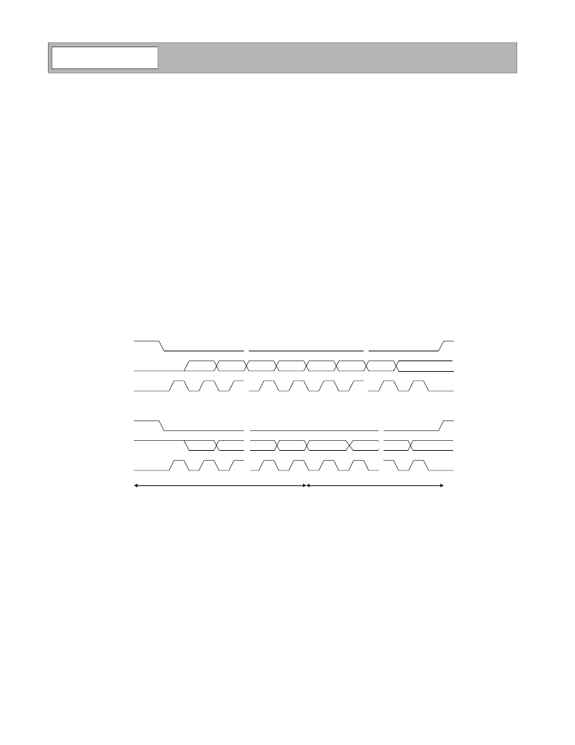
SERIAL DATA INTERFACE
A three wire serial data interface allows user programming of the internal control registers in the RF2958. The serial data
interface consists of the serial select (SSB), serial data in (SDI) and serial clock (SCLK) pins. The SDI is a bi-directional
pin, by default it is configured as an input to the serial interface, but during a read session it is used as an output.
The first bit in a serial transfer (the MSB) is the read/write (R/W) bit. R/W = 1 for a read, and R/W = 0 for a write.
The figure below shows a timing diagram for a serial transfer to the RF2958 serial data interface. The serial select (SSB)
pin is normally high. A serial transfer is initiated by taking SSB low. The address and data bits on the serial data in (SDI)
pin are shifted in on rising edges of the serial clock (SCLK) pin, MSB first. The data is latched and changes take effect on
the falling edge of the clock pulse corresponding to the last (18
th
) data bit in the addressed register. If the transfer is inter-
rupted, such that the 18
th
data bit clock pulse does not occur, then no data is written to the register.
When the synthesizers are programmed, an internal pulse is generated alerting the synthesizer that a new setting is
required. In order to guarantee that this internal pulse is long enough, the time between the falling edge of the last serial
clock pulse and the rising edge of SSB must be at least 1/fr.
The RF2958 can be reset to its power on condition (including register defaults) by writing ‘011111b’ plus 18 don’t care
bits to the serial data interface. The reset is actually performed when the SSB is raised after the write. Although this com-
mand can be performed during any settings of the MODE0 and MODE1 pins, care should be taken to ensure that the
registers are reprogrammed in a sufficient time to perform any transmit or receive operations.
rw=1
addr4
addr3
addr1
addr0
data17
data16
data1
data0
Serial Write
Serial Read
sdi pin direction - input
sdi pin direction - output
addr4
addr3
addr1
addr0
data17
data16
data1
data0
rw=0
SSB
SDI
SCLK
SSB
SCLK
SDI
相關(guān)PDF資料 |
PDF描述 |
|---|---|
| RF2958TR13 | 2.4GHz SPREAD-SPECTRUM TRANSCEIVER |
| RF2968 | BLUETOOTHTM TRANSCEIVER |
| RF3160 | DUAL-BAND GSM/DCS POWER AMP MODULE |
| RF3160PCBA | DUAL-BAND GSM/DCS POWER AMP MODULE |
| RF3164 | 3V 1900MHz LINEAR POWER AMPLIFIER MODULE |
相關(guān)代理商/技術(shù)參數(shù) |
參數(shù)描述 |
|---|---|
| RF2958TR13 | 制造商:RFMD 制造商全稱:RF Micro Devices 功能描述:2.4GHz SPREAD-SPECTRUM TRANSCEIVER |
| RF2959-000 | 制造商:TE Connectivity 功能描述:GAS TUBE 5MM 600V 20% 5KA SMD |
| RF2960-000 | 制造商:TE Connectivity 功能描述:GAS TUBE 8MM 800V 15% 5KA AXIAL |
| RF2961-000 | 制造商:TE Connectivity 功能描述:GAS TUBE 5MM 420V 20% 2.5KA SMD |
| RF2968 | 制造商:RFMD 制造商全稱:RF Micro Devices 功能描述:BLUETOOTHTM TRANSCEIVER |
發(fā)布緊急采購,3分鐘左右您將得到回復(fù)。