- 您現(xiàn)在的位置:買(mǎi)賣(mài)IC網(wǎng) > PDF目錄385769 > RF2926 (RF MICRO DEVICES INC) UHF DUAL CONVERSION TRANSCEIVER PDF資料下載
參數(shù)資料
| 型號(hào): | RF2926 |
| 廠商: | RF MICRO DEVICES INC |
| 元件分類(lèi): | 通信及網(wǎng)絡(luò) |
| 英文描述: | UHF DUAL CONVERSION TRANSCEIVER |
| 中文描述: | SPECIALTY TELECOM CIRCUIT, PQFP48 |
| 封裝: | PLASTIC, LQFP-48 |
| 文件頁(yè)數(shù): | 4/10頁(yè) |
| 文件大小: | 327K |
| 代理商: | RF2926 |
11-188
RF2926
Rev A5 010404
11
T
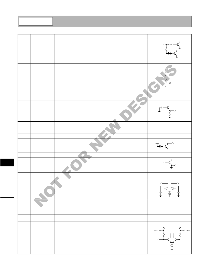
Pin
1
Function
TX ENABL
Description
Enables the transmitter circuits. TX ENABL>2.0V powers up all trans-
mitter functions. TX ENABL<1.0V turns off all transmitter functions
except the PLL functions.
Interface Schematic
2
TX OUT
RF output pin for the transmitter electronics. TX OUT output impedance
is a low impedance (see output impedance plot in Figure TBD) when
the transmitter is enabled. TX OUT is a high impedance when the
transmitter is disabled.
3
GND2
Ground connection for the 40 dB IF limiting amplifier and Tx PA func-
tions. Keep traces physically short and connect immediately to ground
plane for best performance.
RF input pin for the receiver electronics. RX IN input impedance is a
low impedance (see input impedance plot in Figure TBD) when the
receiver is enabled. RX IN is a high impedance when the receiver is
disabled.
4
RX IN
5
GND1
Ground connection for RF receiver functions. Keep traces physically
short and connect immediately to ground plane for best performance.
Ground connection for the LNA.
6
7
8
LNA GND
LNA GND
LNA OUT
Ground connection for the LNA.
Output pin for the receiver RF low noise amplifier. This pin is an open
collector output and requires an external pull up coil to provide bias and
tune the LNA output. A capacitor in series with this output can be used
to match the LNA to 50
impedance image filters.
Same as pin 4.
9
10
GND3
MIX IN
RF input to the RF Mixer. An LC matching network between LNA OUT
and MIX IN can be used to connect the LNA output to the RF mixer
input in applications where an image filter is not needed or desired.
11
GND5
GND5 is the ground connection shared by the input stage of the trans-
mit power amplifier and the receiver RF mixer.
Complementary (with respect to pin 13) IF output from the RF mixer.
Alternately, an IF tank can be used to tailor the IF frequency and band-
width to meet the needs of a given application.
12
MIX OUT+
13
MIX OUT-
IF output from the RF mixer. For a balanced mixer output, pull-up induc-
tors from pin 12 and 13 to V
CC
and a capacitor between the pins should
be used. The sum of the total pull-up inductance should be used to res-
onate the capacitor between pins 12 and 13.
DC feedback node for the 40dB limiting amplifier strip. A 10nF bypass
capacitor from this pin to ground is required.
IF input to the 40dB limiting amplifier strip. A DC blocking capacitor is
required on this input. The value of this capacitor should be small
enough as to not attenuate the IF frequency when terminated into the
330
input impedance.
See pin 12.
14
IF1 BP+
See pin 16.
15
IF1 IN
40 k
20 k
TX ENABL
TX OUT
20
V
CC
RX IN
500
LNA OUT
V
CC
GND5
MIX IN
MIX OUT-
MIX OUT+
15 pF
15 pF
GND5
GND5
IF1 IN+
330
330
60 k
60 k
IF1 BP+
IF1 BP-
相關(guān)PDF資料 |
PDF描述 |
|---|---|
| RF2938 | 2.4GHZ SPREAD-SPECTRUM TRANSCEIVER |
| RF2942 | UHF QUADRATURE MODULATOR AND TRANSMITTER |
| RF2945 | 433/868/915MHZ FSK/ASK/OOK TRANSCEIVER |
| RF2958 | 2.4GHz SPREAD-SPECTRUM TRANSCEIVER |
| RF2958PCBA | 2.4GHz SPREAD-SPECTRUM TRANSCEIVER |
相關(guān)代理商/技術(shù)參數(shù) |
參數(shù)描述 |
|---|---|
| RF2926-000 | 制造商:TE Connectivity 功能描述:FEMTOSMDC005F-2 - Tape and Reel |
| RF2926PCBA | 制造商:RFMD 制造商全稱(chēng):RF Micro Devices 功能描述:UHF DUAL CONVERSION TRANSCEIVER |
| RF2938 | 制造商:RF Micro Devices Inc 功能描述:Telecommunication IC |
| RF2938TR13 | 制造商:未知廠家 制造商全稱(chēng):未知廠家 功能描述:Interface IC |
| RF2942 | 制造商:RFMD 制造商全稱(chēng):RF Micro Devices 功能描述:UHF QUADRATURE MODULATOR AND TRANSMITTER |
發(fā)布緊急采購(gòu),3分鐘左右您將得到回復(fù)。