- 您現(xiàn)在的位置:買賣IC網(wǎng) > PDF目錄376305 > REG102 (Texas Instruments, Inc.) DMOS 250mA Low-Dropout Regulator PDF資料下載
參數(shù)資料
| 型號: | REG102 |
| 廠商: | Texas Instruments, Inc. |
| 英文描述: | DMOS 250mA Low-Dropout Regulator |
| 中文描述: | 的DMOS 250mA的低壓差穩(wěn)壓器 |
| 文件頁數(shù): | 13/19頁 |
| 文件大小: | 342K |
| 代理商: | REG102 |

REG102
SBVS024E
13
www.ti.com
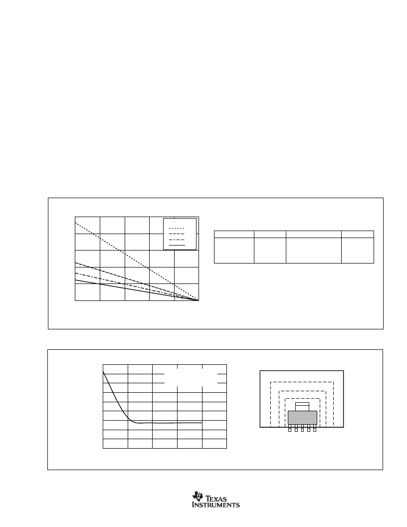
FIGURE 7. Maximum Power Dissipation versus Ambient Temperature for the Various Packages and PCB Heat Sink Configurations.
FIGURE 8. Thermal Resistance versus PCB Area for the Five Lead SOT-223.
THERMAL RESISTANCE vs PCB COPPER AREA
180
160
140
120
100
80
60
40
20
0
T
J
°
C
θ
0
1
2
3
4
5
Copper Area (inches
2
)
Circuit-Board Copper Area
REG102
SOT-223 Surface-Mount Package
REG102
Surface-Mount Package
1 oz. copper
2.5
2
1.5
1
0.5
0
P
0
25
50
75
125
100
Ambient Temperature (
°
C)
DEVICE DISSIPATION vs TEMPERATURE
CONDITION
1
2
3
4
PACKAGE
SOT-223
SOT-223
SO-8
SOT-23
PCB AREA
4in2 Top Side Only
0.5in2 Top Side Only
—
—
THETA J-A
53
°
C/W
110
°
C/W
150
°
C/W
200
°
C/W
CONDITIONS
#1
#2
#3
#4
POWER DISSIPATION
The REG102 is available in three different package configu-
rations. The ability to remove heat from the die is different for
each package type and, therefore, presents different consid-
erations in the printed circuit-board layout. The PCB area
around the device that is free of other components moves the
heat from the device to the ambient air. Although it is difficult
to impossible to quantify all of the variables in a thermal
design of this type, performance data for several simplified
configurations are shown in Figure 7. In all cases, the PCB
copper area is bare copper (free of solder resist mask), not
solder plated, and are for 1-ounce copper. Using heavier
copper will increase the effectiveness in moving the heat
from the device. In those examples where there is copper on
both sides of the PCB, no connection has been provided
between the two sides. The addition of plated through holes
will improve the heat sink effectiveness.
Power dissipation depends on input voltage, load conditions,
and duty cycle and is equal to the product of the average
output current times the voltage across the output element,
V
IN
to V
OUT
voltage drop.
P
V
V
I
D
IN
OUT
OUT
=
(
–
)
(3)
Power dissipation can be minimized by using the lowest
possible input voltage necessary to assure the required
output voltage.
REGULATOR MOUNTING
The tab of the SOT-223 package is electrically connected to
ground. For best thermal performance, this tab must be
soldered directly to a circuit-board copper area. Increasing
the copper area improves heat dissipation, as shown in
Figure 8.
Although the tab of the SOT-223 is electrical ground, it is not
intended to carry current. The copper pad that acts as a heat
sink should be isolated from the rest of the circuit to prevent
current flow through the device from the tab to the ground
pin. Solder pad footprint recommendations for the various
REG102 devices are presented in Application Bulletin Solder
Pad Recommendations for Surface-Mount Devices
(SBFA015), available from the Texas Instruments web site
(www.ti.com).
相關(guān)PDF資料 |
PDF描述 |
|---|---|
| REG113 | DMOS 400mA Low-Dropout Regulator(DMOS 400mA 低壓差穩(wěn)壓器) |
| REG5601 | 18-Line SCSI Active Terminator(18線SCSI有源終端) |
| REG5608 | Low Capacitance 18-Line SCSI Active Terminator(低電容的18線SCSI有源終端) |
| REG710 | 60MA SWITCHED CAP BUCK/BOOST CONVERTER |
| REJ03C0098_R1LV0408C | Wide Temperature Range Version 4M SRAM (512-kword 】 8-bit) |
相關(guān)代理商/技術(shù)參數(shù) |
參數(shù)描述 |
|---|---|
| REG102_07 | 制造商:BB 制造商全稱:BB 功能描述:DMOS 250mA Low-Dropout Regulator |
| REG102_08 | 制造商:BB 制造商全稱:BB 功能描述:DMOS 250mA Low-Dropout Regulator |
| REG102-25 | 制造商:未知廠家 制造商全稱:未知廠家 功能描述:DMOS 250 mA Low Dropout (LDO) Regulator |
| REG102-28 | 制造商:未知廠家 制造商全稱:未知廠家 功能描述:DMOS 250 mA Low Dropout (LDO) Regulator |
| REG102-285 | 制造商:未知廠家 制造商全稱:未知廠家 功能描述:DMOS 250 mA Low Dropout (LDO) Regulator |
發(fā)布緊急采購,3分鐘左右您將得到回復(fù)。