- 您現(xiàn)在的位置:買賣IC網(wǎng) > PDF目錄376305 > REF08 (Texas Instruments, Inc.) Make a Precision -10V Reference(使用精密-10V電壓基準) PDF資料下載
參數(shù)資料
| 型號: | REF08 |
| 廠商: | Texas Instruments, Inc. |
| 英文描述: | Make a Precision -10V Reference(使用精密-10V電壓基準) |
| 中文描述: | 制作精密10V的參考(使用精密- 10V的電壓基準) |
| 文件頁數(shù): | 1/2頁 |
| 文件大小: | 29K |
| 代理商: | REF08 |

5
6
7
8
10
11
12
13
14
15
9
3
1
4
2
The need for a precision –10.0V reference arises often. For
example, the best way to get a 0V to +10V output from a
CMOS MDAC is to use a –10V reference (see Figures 4-6).
ADI/PMI has the REF-08 –10V reference, but it has limited
performance. Although Burr-Brown offers no –10V refer-
ence, the REF102 precision +10.0V reference can be accu-
rately converted to a precision –10.0V reference. The circuit
is simple and requires no precision components. The 2.5ppm/
°
C temperature drift of the Burr-Brown REF102 is twenty
times better than the 50ppm/
°
C best grade of the PMI REF-
08. (Even our lowest grade is five times better.)
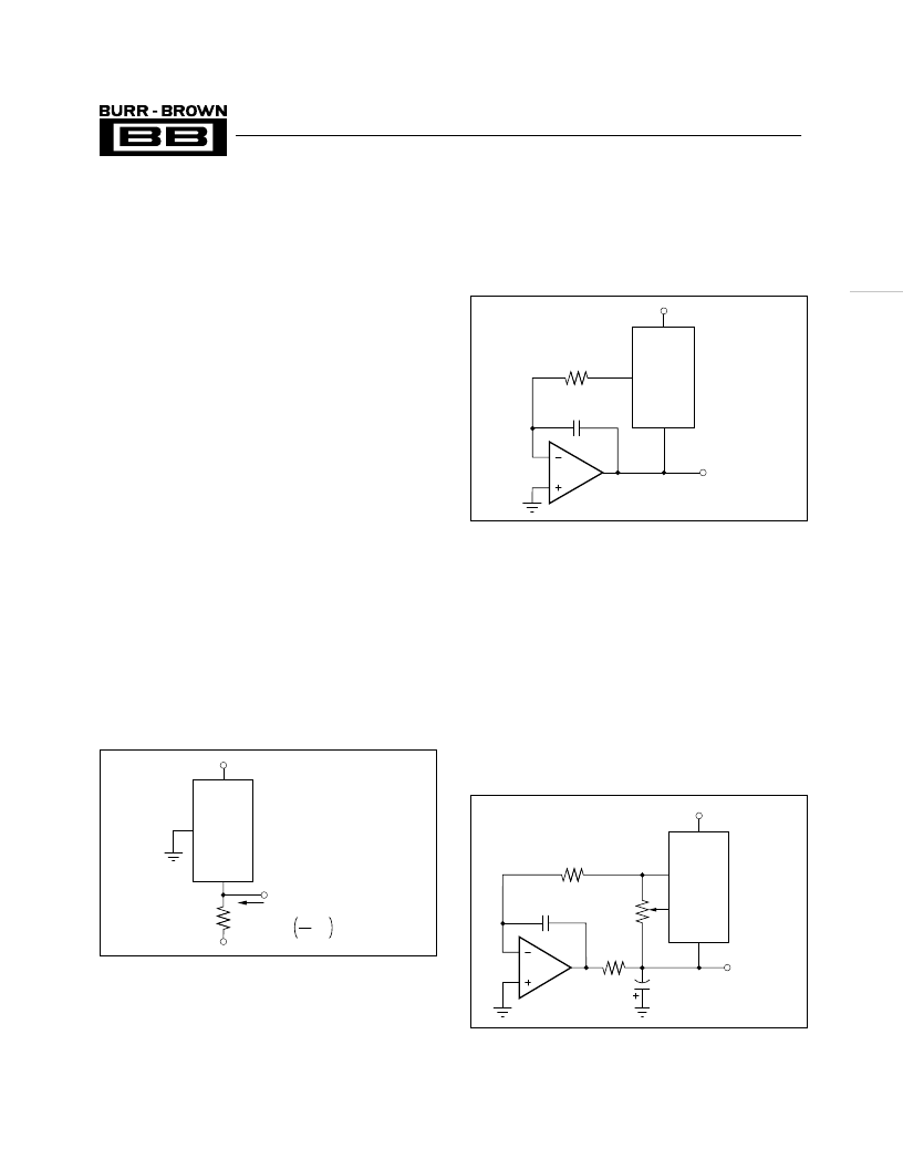
The simplest approach for converting a REF102 into a
–10.0V reference is shown in Figure 1. The only extra
component is a 1k
resistor connected to –V
S
. This circuit
is useful, but has limitations. Maximum expected load cur-
rent plus maximum reference quiescent current must be
supplied by the resistor at minimum –V
S
. Changes in current
resulting from load and power supply variations must be
driven by the reference. The excess current through the
reference reduces its accuracy due to drift from self-heating
and thermal feedback. Changes in reference output current
due to power-supply variations translate into line regulation
error. Voltage reference load regulation is not usually as
good as line regulation. Finally, the output impedance due to
the resistor pull-down causes settling problems with dy-
namic loads.
FIGURE 2. Improved –10V Reference.
To understand how the circuit works, notice that the refer-
ence is in the feedback loop of the op amp. The op amp
output forces the Gnd connection of the reference to exactly
–10.0V so that the voltage at the op amp inverting input is
the same as at its noninverting input (ground). Since no
current flows into the op amp input, the reference output
current remains at zero, eliminating voltage reference ther-
mal feedback or load regulation errors. The R
1
, C
1
network
assures loop stability and provides noise filtering. Reference
noise is filtered by a single pole of f
–3dB
= 1/(2
π
R
1
C
1
).
Bias current flowing through R
1
can produce DC errors and
noise. If a lower filter pole is needed, keep R
1
= 2k
and
increase C
1
to preserve accuracy.
FIGURE 3. Improved –10V Reference with Improved Filter,
with V
OUT
Trim.
FIGURE 1. Simple –10V Reference.
The circuit shown in Figure 2 solves these problems. As in
Figure 1, no precision resistors are needed. The error con-
tributed by the op amp is negligible (the OPA27 0.6
μ
V/
°
C
V
OS
/dT
adds only 0.06 ppm/
°
C drift to the –10V reference).
As a bonus, the circuit incorporates noise filtering.
MAKE A PRECISION –10V REFERENCE
By R. Mark Stitt (520) 746-7445
–10V Out
+V (1.4V to 26V)
2
6
4
10V
Out
Gnd
V+
REF102
OPA27
R
1
2k
C
1000pF
–10V Out
+V (1.4V to 26V)
2
6
4
10V
Out
Gnd
V+
REF102
OPA27
R
1
2k
C
0.05μF
Trim
5
20k
R
2
50
C
1.0μF
Tantalum
R
S
1k
I
L
–10V Out
+V (1.4V to 26V)
2
6
4
10V
Out
Gnd
V+
REF102
–15V
1.4 < R
S
5V
L
APPLICATION BULLE TIN
Mailing Address: PO Box 11400 Tucson, AZ 85734 Street Address: 6730 S. Tucson Blvd. Tucson, AZ 85706
Tel: (520) 746-1111 Twx: 910-952-111 Telex: 066-6491 FAX (520) 889-1510 Immediate Product Info: (800) 548-6132
1990 Burr-Brown Corporation
AB-004B
Printed in U.S.A. June, 1995
相關PDF資料 |
PDF描述 |
|---|---|
| REF10 | Precision Voltage Reference(精密電壓基準) |
| REG101 | DMOS 100mA Low-Dropout Regulator |
| REG102UA-2.8 | DMOS 250mA Low-Dropout Regulator |
| REG102UA-2.85 | DMOS 250mA Low-Dropout Regulator |
| REG102GA-2.8 | DMOS 250mA Low-Dropout Regulator |
相關代理商/技術參數(shù) |
參數(shù)描述 |
|---|---|
| REF10 | 制造商:BB 制造商全稱:BB 功能描述:Precision VOLTAGE REFERENCE |
| REF100-11/12 | 功能描述:鼓風機 Size=100x25 mm CFM=50.6 VDC=12 RoHS:否 制造商:Murata 產(chǎn)品:Blowers 電流類型:DC 電源電壓:5.3 V 氣流:1 l/min 軸承類型: 噪聲: 速度: 功率額定值: 框架尺寸 (mm):20 mm x 20 mm x 1.85 mm 外殼材料: 端接類型:SMD/SMT 系列:MZB |
| REF100-11/12/17U-202 | 功能描述:鼓風機 FLATPAK - RAD BLOWR RoHS:否 制造商:Murata 產(chǎn)品:Blowers 電流類型:DC 電源電壓:5.3 V 氣流:1 l/min 軸承類型: 噪聲: 速度: 功率額定值: 框架尺寸 (mm):20 mm x 20 mm x 1.85 mm 外殼材料: 端接類型:SMD/SMT 系列:MZB |
| REF100-11/12/2 | 功能描述:鼓風機 FlatPak - Radial Blower RoHS:否 制造商:Murata 產(chǎn)品:Blowers 電流類型:DC 電源電壓:5.3 V 氣流:1 l/min 軸承類型: 噪聲: 速度: 功率額定值: 框架尺寸 (mm):20 mm x 20 mm x 1.85 mm 外殼材料: 端接類型:SMD/SMT 系列:MZB |
| REF100-11/12/2PU-210 | 制造商:ebm-papst Inc 功能描述:- Bulk |
發(fā)布緊急采購,3分鐘左右您將得到回復。