- 您現(xiàn)在的位置:買賣IC網(wǎng) > PDF目錄230922 > RDC-19220S-422K (DATA DEVICE CORP) SYNCHRO OR RESOLVER TO DIGITAL CONVERTER, CDIP40 PDF資料下載
參數(shù)資料
| 型號(hào): | RDC-19220S-422K |
| 廠商: | DATA DEVICE CORP |
| 元件分類: | 位置變換器 |
| 英文描述: | SYNCHRO OR RESOLVER TO DIGITAL CONVERTER, CDIP40 |
| 封裝: | 2 X 0.600 INCH, 0.200 INCH HEIGHT, CERAMIC, DDIP-40 |
| 文件頁(yè)數(shù): | 6/20頁(yè) |
| 文件大?。?/td> | 276K |
| 代理商: | RDC-19220S-422K |
第1頁(yè)第2頁(yè)第3頁(yè)第4頁(yè)第5頁(yè)當(dāng)前第6頁(yè)第7頁(yè)第8頁(yè)第9頁(yè)第10頁(yè)第11頁(yè)第12頁(yè)第13頁(yè)第14頁(yè)第15頁(yè)第16頁(yè)第17頁(yè)第18頁(yè)第19頁(yè)第20頁(yè)
14
Data Device Corporation
www.ddc-web.com
RDC-19220/2S
E-11/02-300
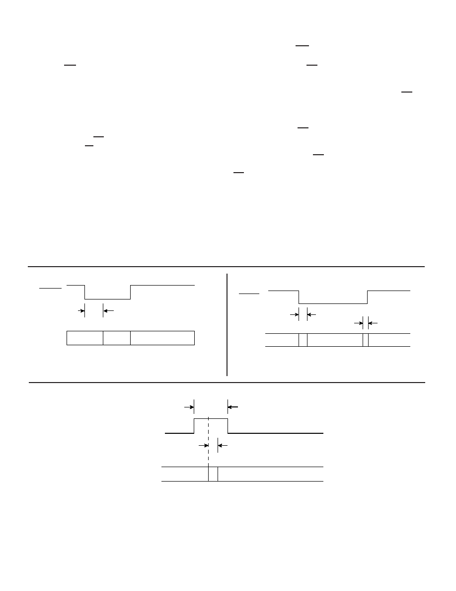
INHIBIT, ENABLE, AND CB TIMING
The Inhibit (INH) signal is used to freeze the digital output angle
in the transparent output data latch while data is being trans-
ferred. Application of an inhibit signal does not interfere with the
continuous tracking of the converter. As shown in FIGURE 13,
angular output data is valid 150 ns maximum after the applica-
tion of the negative inhibit pulse.
Output angle data is enabled onto the tri-state data bus in two
bytes. Enable MSBs (EM) is used for the most significant 8 bits
and Enable LSBs (EL) is used for the least significant 8 bits. As
shown in FIGURE 14, output data is valid 150 ns maximum after
the application of a negative enable pulse. The tri-state data bus
returns to the high impedance state 100 ns maximum after the
rising edge of the enable signal.
The Converter Busy (CB) signal indicates that the tracking con-
verter output angle is changing 1 LSB. As shown in FIGURE 15,
output data is valid 50 ns maximum after the middle of the CB
pulse. The CB pulse width is 1/40 Fs, which is nominally 375 ns.
BUILT-IN-TEST (BIT)
The Built-ln-Test output (BIT) monitors the level of error from the
demodulator. This signal is the difference in the input and output
angles and ideally should be zero; if it exceeds approximately
100 LSBs (of the selected resolution) the logic level at BIT will
change from a logic 1 to a logic 0.
This condition will occur during a large step and reset after the
converter settles out. BIT will also change to logic 0 for an over-
velocity condition, because the converter loop cannot maintain
input-output or if the converter malfunctions where it cannot
maintain the loop at a null. BIT will also be set low for a detected
Loss-of-Signal (LOS) and/or a Loss-of-Reference (LOR). The
BIT signal may pulse during certain error conditions, i.e., when
the converter is in a spin around condition or the signal amplitude
is on the threshold of LOS.
LOS will be detected if both sin and cos input voltages are less
than 500 mV peak. LOR will be detected if the differential refer-
ence voltage is less than 500 mV peak.
;;
;;;
DATA
VALID
150 ns max
INHIBIT
;
100 ns MAX
ENABLE
150 ns MAX
DATA
VALID
HIGH Z
;
1/40 FS
(375 nsec nominal)
CB
50 ns
DATA
VALID
DATA
VALID
FIGURE 13. INHIBIT TIMING
FIGURE 14. ENABLE TIMING
FIGURE 15. CONVERTER BUSY TIMING
相關(guān)PDF資料 |
PDF描述 |
|---|---|
| RDC-19220S-422L | SYNCHRO OR RESOLVER TO DIGITAL CONVERTER, CDIP40 |
| RD-14597F1-234L | SYNCHRO OR RESOLVER TO DIGITAL CONVERTER, CDFP36 |
| RD-14591D1-434 | SYNCHRO OR RESOLVER TO DIGITAL CONVERTER, MDMA36 |
| RDC-19223-122 | SYNCHRO OR RESOLVER TO DIGITAL CONVERTER, CDIP40 |
| RDC-19221-201 | SYNCHRO OR RESOLVER TO DIGITAL CONVERTER, PDIP28 |
相關(guān)代理商/技術(shù)參數(shù) |
參數(shù)描述 |
|---|---|
| RDC19221-101 | 制造商:未知廠家 制造商全稱:未知廠家 功能描述:Converter IC |
| RDC-19221-102 | 制造商:未知廠家 制造商全稱:未知廠家 功能描述:LVDT/Resolver-to-Digital Converter |
| RDC-19221-103 | 制造商:未知廠家 制造商全稱:未知廠家 功能描述:LVDT/Resolver-to-Digital Converter |
| RDC19221-121 | 制造商:未知廠家 制造商全稱:未知廠家 功能描述:Converter IC |
| RDC-19221-122 | 制造商:未知廠家 制造商全稱:未知廠家 功能描述:LVDT/Resolver-to-Digital Converter |
發(fā)布緊急采購(gòu),3分鐘左右您將得到回復(fù)。